Description
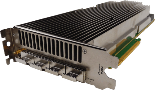
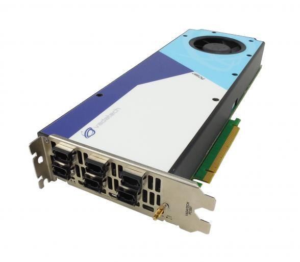
The PCI597 is based on the Xilinx VU13P UltraScale+TM FPGA, which provides over 12,000 DSP slices, 360 Mb of UltraRAM and 3,780K logic cells. The Unit provides active cooling of the FPGA making it appropriate for power-hungry applications or those requiring temperature stability for good performance. The FPGA has interface to dual DDR4 memory channels (dual bank of 64-bit wide, 32 GB total). This allows for large buffer sizes to be stored during processing as well as for queuing the data to the host.
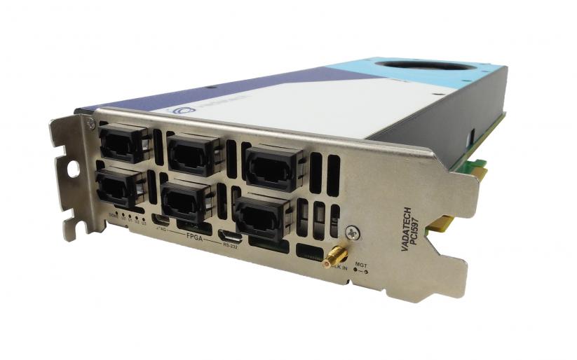
Front panel I/O is via six Board-Mount Optical Assemblies, each providing 12 channel full-duplex transceivers with Clock Data Recovery (CDR*) and fiber I/O via MTP/MPO. Transceivers are available in two speed grades, 10.6 Gb/s and 28.1 Gb/s per channel, both with multi-rate capability. The 10.6 Gb/s can drive 100 m over OM3 MM Fiber and 28.1 Gb/s can drive 100 m over the OM4 MM Fiber. The high number of egress ports allows the single FPGA to be the central point of data gathering.
The PCI597 has x16 PCIe edge connector routed to the FPGA PCIe Gen3 hard IP block. Further, the module has an addition PCIe x16 hard core which takes a second PCIe x16 slot in the chassis that allows pushing/pulling data into the host as an aggregated x32 PCIe. See PCI124 for details
Reference Design
VadaTech provides a reference design implementation for our FPGAs, complete with VHDL source code and configuration binaries. The reference design focuses on the I/O ring of the FPGA to demonstrate low-level operation of the interconnections between the FPGA and other circuits on the board and/or backplane. It is intended to prove-out the hardware for engineering/factory diagnostics and customer acceptance, and can be used as a starting point for developing an end application.
*CDR applies only to the 28G optics not the 10G optics