Description
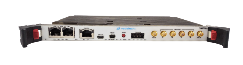
The VME599 provides dual ADC sampling rates of up to @6.4GSPS at a 12-bit resolution TI ADC12DJ3200 or quad inputs at @3.2GSPS (or dual ADC12DJ2700 for two channels @5.4GSPS or four channels @2.7GSPS).
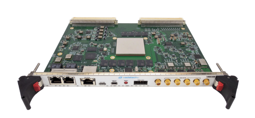
The unit has an onboard, re-configurable UltraScale+™ XCKU115 FPGA that directly interfaces with ADC and three banks of DDR4 memory channels. This allows for large buffer sizes to be stored during processing as well as for queuing the data to the host. The Dual 64-bit wide DDR-4 bank has total of 16 GByte and the single bank of 32-bit DDR-4 has 4GByte
The VME599 have on board wide-band PLL which provides the RF sampling clock to the ADC parts (both ADC receive the same sampling clock). This PLL can lock into an external clock and has hitless switching and holdover between the two input clocks.
The module has dual 10GbE and single GbE to the FPGA. This allows digitized data to be transferred in real time to external host.
The on-board quad core ARM processor provides flexibility to monitor an manage the FPGA. The CPU can load the FPGA image via PCIe. The onboard CPU monitors all the temperature sensors which can provide real time data to an external host. The CPU has 4GByte of memory as well and SDHC socket and a 64GByte of Flash to boot and store data.
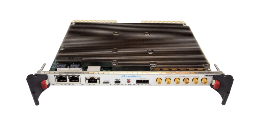
The module takes power from P1 but does not implement VME bus transactions. Further from the FPGA there is 40 LVDS pairs that are routed to P0.
This makes VME599 suitable for signal capture/analysis applications such as COMINT/SIGINT, radar, research and instrumentation.