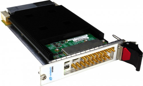
Description
The VPX540 provides 20 ADC @ 4GSPS with 16 DAC @ 12GSPS with 14-bit resolution with integrated FPGA and quad Core ARM Cortex-A53 as a System on Chip (SoC). The ADC/DAC have a front-end RF bandwidth of 7.125 GHz. The module has 24GB of the DDR-4 memory to the FPGA as three banks of 8GB 64-bit wide each with the ECC. To the ARM there is single bank of 4GB of 32-bit wide DDR-4 memory with ECC.
The FPGA interfaces directly to rear I/O via high-speed SERDES, supporting PCIe, SRIO, Ethernet (1G/10G/25G/50G/100G/200G/400G), and/or Serial Lite backplane connections. General purpose I/O signals and LVDS are also routed to the rear. The front panel contains a total of 12 status and user-defined LEDs. All the RF connections are thru the front panel via SSMC (38 total). The module’s front panel also has a QSFP-DD (Quad Small Form Factor Pluggable Double Density) egress port which can go up to 400G.
The on-board PLL can lock into the incoming clock for synchronizing to an external clock and provides synchronized clocks to the ADC/DAC for the RF sampling. The sampling on the ADC/DAC are fully coherent with each other.
The module has capability to synchronize across multiple modules within the chassis. This allows digital beam forming for phased array radar. The module could be used for other applications such as SAR (Synthetic Aperture Radar), EW/ECM Jamming, Military Communication System as well as Military COTS Digitizer.
The VPX540 includes platform health management/monitoring capability using VadaTech’s field-proven IPMI software as Tier-2 support per VITA 46.11.
The unit is available in a range of temperature and shock/vibe specifications per ANSI/VITA 47, up to V3 and OS2. The module follows the SOSA specification for its rear I/O to the backplane.