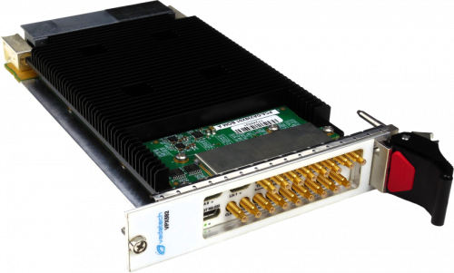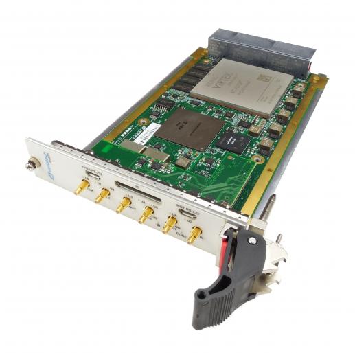
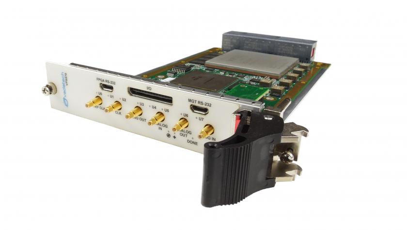
Description
The VPX570 provides an ADC with sampling rates of up to 5.4 GSPS at a 12-bit resolution (EV12AS350A) and a DAC that delivers update rates of up to 6 GSPS also at a 12-bit resolution (EV12DS460A). Both Converters have parallel interface to the FPGA, avoiding latency associated with serializing/deserializing data.
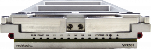
The XCVU13P FPGA has large 360 Mb on-chip UltraRAM which, with the ADC and DAC selection, makes this module ideal for low-latency applications such as DRFM, radar simulators and smart jammers. The FPGA interfaces directly to rear I/O via SERDES and LVDS, supporting PCIe, SRIO, GbE/10GbE/40GbE or Aurora backplane connections. General purpose I/O signals, e.g. for trigger, are routed to the front panel that also contains 8 LED/Bi-color.
ADC and DAC have a common sampling clock, which can be fed from front panel (Direct RF Clock) or from PLL locked to a 10/100 MHz reference clock sourced from front panel or backplane. Sampling clock selection is by ordering option.
The VPX570 includes platform health management/monitoring capability using VadaTech’s field-proven IPMI software. An onboard management controller has the ability to access board sensors and manage FPGA image updates.
The unit is available in a range of temperature and shock/vib specifications per ANSI/VITA 47, up to V3 and OS2.
VadaTech’s Multi-Path Modulation software package can provide an additional FPGA image and source code for the VPX570, See Datasheet MPM_VPX570 and Video MPM570 Development Accelerator for details.
* Also view our VIDEO and DATASHEET on MPM570, our Development Accelerator “MultiPath Modulation” Software Package.