FMC215

FMC ADC 12-bit @ 4.0 GSPS and DAC 12-bit @ 4.5 GSPS

  • FPGA Mezzanine Card (FMC) per VITA 57.1
  • TI ADC12J4000 12-bit ADC supports 1-4 GSPS with a full-power input bandwidth of 3.2 GHz
  • E2V EV12DS400 12-bit DAC supports up to 4.5 GSPS with output bandwidth 7 GHz
  • Excellent dynamic performance
  • Front panel interface includes CLK In, Trig In, AnalogIn/Out, and GPIO
  • Ultra-Low Noise Wideband PLL
  • On-chip delay locked loops (DLLs) optimize timing between different clock domains.

Download Datasheet Add to Info Request

add to compare
0

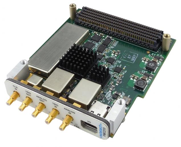
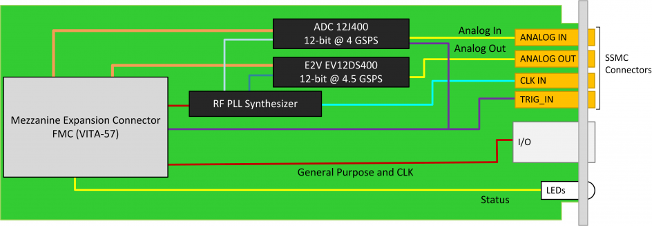
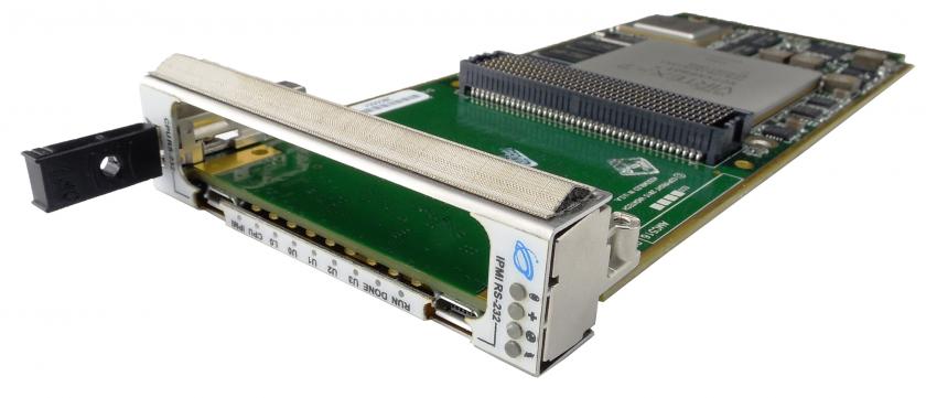
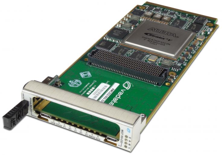
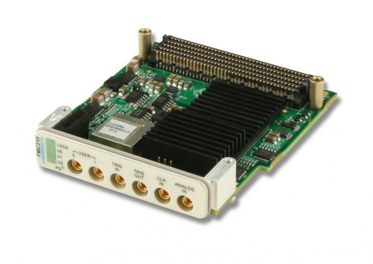
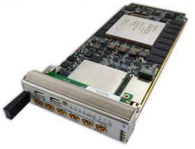
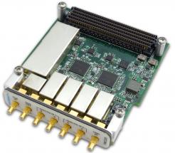
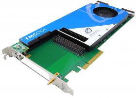
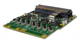
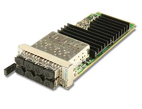
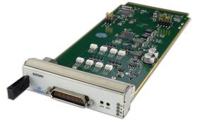
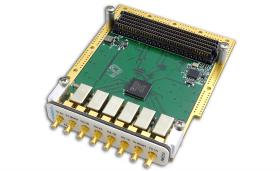
The FMC215 is an FPGA Mezzanine Module per VITA 57 specification that provides a single ADC at 4 GSPS and a single DAC at 4.5 GSPS. The module is suitable for signal capture and low-latency feedback applications such as COMINT/SIGINT, radar, jamming, research and instrumentation.

TI ADC12J4000 ADC provides:

  • Usable output bandwidth of 800 MHz at 4x decimation and 4000 MSPS
  • Usable output bandwidth of 100 MHz at 32x decimation and 4000 MSPS
  • Bypass Mode for full Nyquist output bandwidth

E2V EV12DS400 DAC provides:

  • –3 dB Analog output Bandwidth of 7 GHz
  • 1st Nyquist NPR = 47.5 dB, 9.4-bit Equivalent at Fs = 4.5 GSPS
  • 2nd Nyquist NPR = 42 dB, 8.5-bit Equivalent at Fs = 4.5 GSPS
  • 3rd Nyquist NPR = 39 dB, 8-bit Equivalent at Fs = 4.5 GSPS

The Module offers the option for an RF sampling clock, accessed via the front panel for both ADC/DAC as disjoint or a common clock.

The FMC215 has a trigger input which is routed to the FMC connector as well as to the ADC.The analog input/output, clock input and trigger inputs are routed via SSMC connectors.

Key Features
  • FPGA Mezzanine Card (FMC) per VITA 57.1
  • TI ADC12J4000 12-bit ADC supports 1-4 GSPS with a full-power input bandwidth of 3.2 GHz
  • E2V EV12DS400 12-bit DAC supports up to 4.5 GSPS with output bandwidth 7 GHz
  • Excellent dynamic performance
  • Front panel interface includes CLK In, Trig In, AnalogIn/Out, and GPIO
  • Ultra-Low Noise Wideband PLL
  • On-chip delay locked loops (DLLs) optimize timing between different clock domains.
Benefits
  • High dynamic range for versatility in video/broadcastrequirements
  • Ideal for Broadband communications systems, Wirelessinfrastructure, LTE, ATE, RADAR/Jamming
  • Strong mil/aero support
  • Electrical, mechanical, software, and system-level expertisein house
  • Full system supply from industry leader
  • AS9100 and ISO9001 certified company
Specifications
Specifications

Block diagram

Related Products

AMC516

Virtex-7 FPGA Carrier for FMC, AMC

  •  AMC FPGA carrier for FMC per VITA-57
  • Xilinx Virtex-7 690T FPGA in FFG-1761 package with optional P2040
  • Supported by DAQ Series™ data acquisition software
  • AMC Ports 12-15 and 17-20 are routed to the FPGA
  • AMC Ports 4-11 are routed to FPGA per AMC.1, AMC.2 and AMC.4 (protocols such as PCIe, SRIO, XAUI, etc. are FPGA programmable)
  • AMC FCLKA, TCLKA, TCLKB, TCLKC and TCLKD are routed
  • Single module, mid-size AMC (full-size optional)
  • Clock jitter cleaner
  • IPMI 2.0 compliant
View product AMC516 Data Sheet

AMC532

Altera Carrier for FMC, Stratix® V (5SGXEA)

  • Single module, mid-size or full-size
  • AMC FPGA based on Altera Stratix® V (5SGXEA) in F1932 package
  • VITA 57.1 FMC HPC Connector (compatible with LPC)
  • AMC Ports 0-15, 17-20 and FMC Ports DP0-9 are routed for high speed SERDES protocols
  • All FMC LA, HA, HB pairs routed bi-directionally
  • High-speed SERDES protocols such as PCIe x4, SRIO, XAUI, 1000Base-X are FPGA programmable
  • Onboard PLL for buffering/multiplying and jitter cleaner (Stratum-3)
  • M-LVDS/LVDS Clock crossbar switch for flexible clock routing
  • 4 GB of DDR3 memory to FPGA (4 channels x 1 GB each)
  • Serial Over LAN (SOL) with hardware RNG
View product AMC532 Data Sheet

FMC210

FMC ADC 10-bit @ 2.6 GSPS Module

  • FPGA Mezzanine Card (FMC) per VITA-57
  • Single ADC EV10AS150B @2.5 GSPS
  • Single module
  • 5 GHz Full Power Input Bandwidth (-3dB)
  • True single core architecture (no calibration required)
  • External Interleaving:Full scale analog input Voltage Span 500mVpp
    • Gain Adjust
    • Offset Adjust
    • Sampling Delay Adjust
  • All front panel input/outputs are via MMCX:
    • Analog Input
    • Reference clock
    • Trig in/out
    • General purpose I/O
  • Super low phase noise RF PLL Synthesizer
View product FMC210 Data Sheet

Info request

Create a list of products to inquire about for more information or quote request.