A/D & D/A

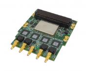
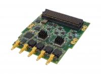
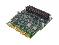
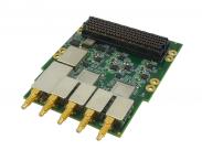
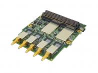
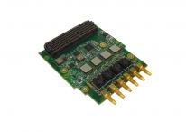
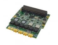
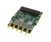
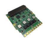
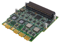
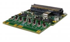
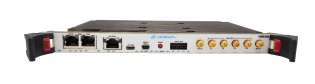
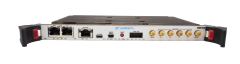
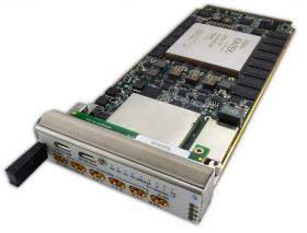
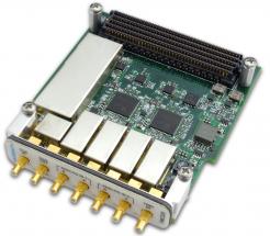
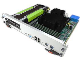
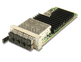
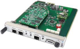
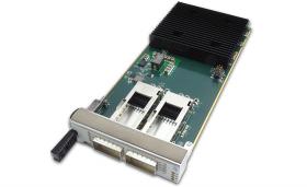
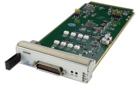
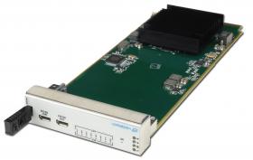
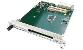
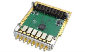
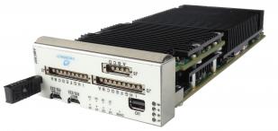
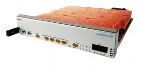
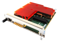
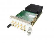
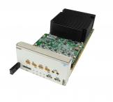
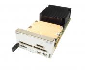
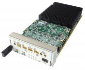
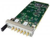
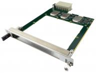
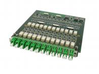
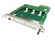
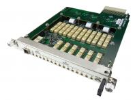
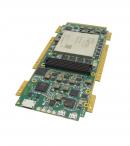
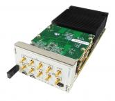
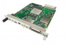
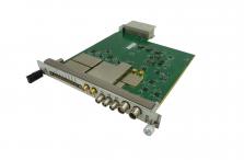
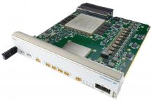
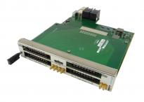
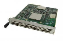
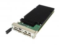
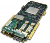
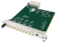
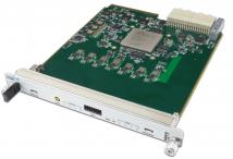
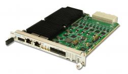
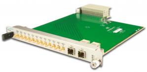
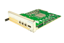
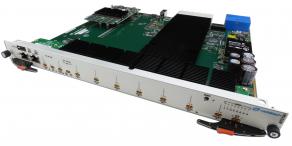
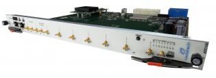
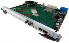
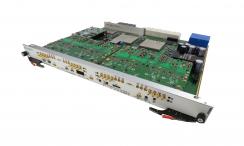
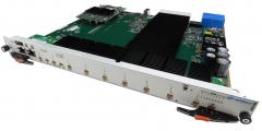
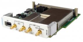
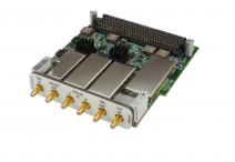
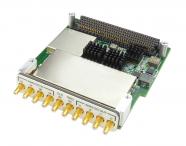
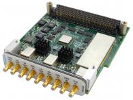
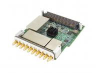
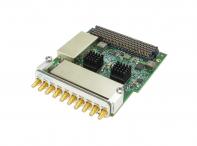
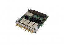
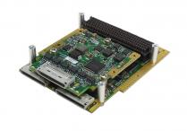
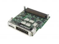
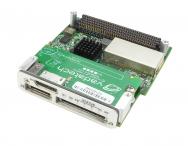
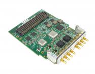
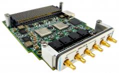
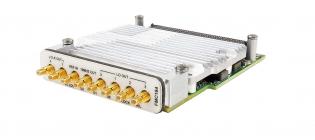
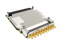
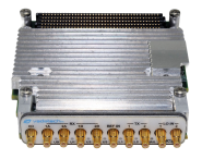
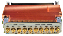
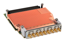
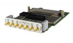
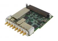
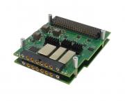
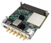
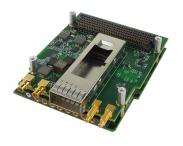
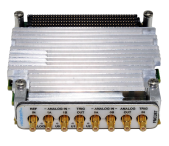
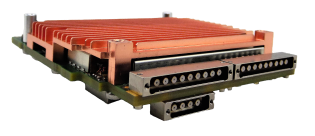
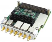
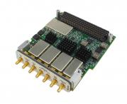
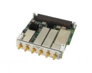
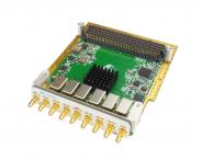
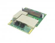
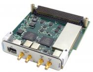
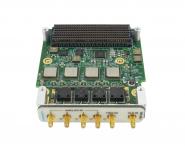
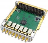
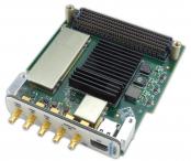
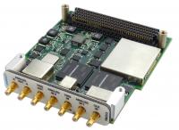
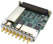
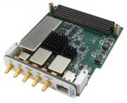
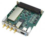
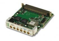
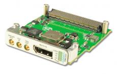
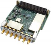
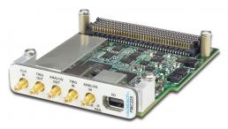
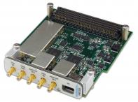
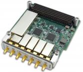
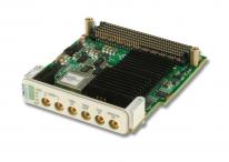
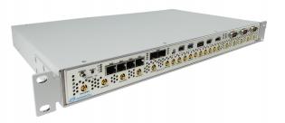
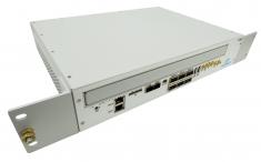
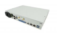
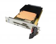
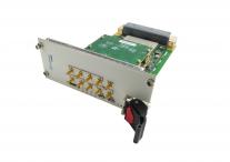
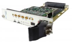
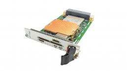
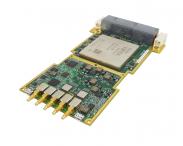
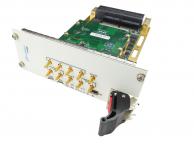
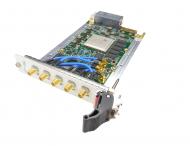
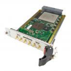
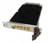
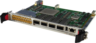
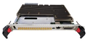
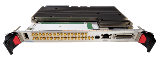
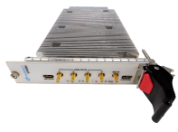
VadaTech has one of the most extensive portfolios of A/D and D/A converters in the industry, in a range of form factors and a variety of channel and sampling rate options to meet all your data acquisition needs. Our ADC and DAC are widely used in high energy physics, military, aerospace and industrial applications thanks to variants based on MicroTCA.4, MicroTCA.0, FMC, OpenVPX and AdvancedTCA (ATCA).


Please contact us if you have any requirements that you don’t see below, our agile R&D team has many years’ experience in developing custom solutions.

AMC FPGA A/D D/A

( close )

AMC597

300 MHz to 6 GHz Octal Versatile Wideband Transceiver (MIMO), UltraScale™, AMC

  • Xilinx UltraScale™ XCKU115 FPGA
  • Octo complete transceiver signal chain solution
  • Four AD9371s or AD9375s on one module
  • Frequency range 300 MHz to 6 GHz
  • Tx synthesis bandwidth (BW) to 250 MHz
  • Rx bandwidth: 8 MHz to 100 MHz
  • Supports Time Division Duplex (TDD) and Frequency Division Duplex (FDD) operation
  • On-board clocking or external clock with multi-transceivers synchronization capability
  • Three banks of DDR4 for total 20 GB
View product AMC597 Data Sheet

AMC549

NEW

SOFI Carrier UltraScale+™

  • Serial Optimized FPGA Interface (SOFI) Carrier
  • Xilinx UltraScale+™ XCVU13P FPGA
  • Dual Tongue to allow additional x16 SERDES routing with x8 additional LVDS on Tongue two
  • Option for high-speed ADC/DAC (see SOFI catalogue) A/D & D/A (vadatech.com)
  • Single bank of DDR4 64-bit wide 8 GB Total
  • AMC Ports 4-11 are routed to FPGA per AMC.1, AMC.2 and AMC.4 (protocols such as PCIe, SRIO, 1/10/40GbE, etc. are FPGA programmable) with additional x16 SERDES on Tongue two
  • AMC FCLKA, TCLKA, TCLKB, TCLKC and TCLKD are routed
  • Clock Jitter cleaner
  • IPMI 2.0 compliant
View product AMC549 Data Sheet

AMC594

LEGACY

Dual ADC 8-bit @ up to 56 GSPS, 2 or 4 Channels, UltraScale™ XCVU190, AMC

  • Dual ADC 8-bit @ up to 56 GSPS
  • 2 x 56 or 4 x 28 GSPS channels
  • Xilinx UltraScale™ XCVU190 FPGA
  • 16 GB of DDR4 Memory (2 banks of 64-bit)
  • ADC is 65 nm CMOS process technology)
  • Double module, full-size
  • Calibration warning and over-range flags
  •  –3 dB analog input bandwidth nominally 15 GHz
  • Internal 14 GHz VCO/PLL per I/Q ADC pair
  • Differential analog input: 1 VPP
View product AMC594 Data Sheet

AMC562

FMC+ Carrier Zynq UltraScale+ FPGA, AMC

  • Xilinx UltraScale+ XCZU7EV FPGA
  • Double module, mid-size
  • FMC+ site
  • 8 GB of 64-bit wide DDR4 Memory (single bank) with ECC
  • SD Card (option)
  • 128 MB of Boot Flash
  • 64 GB of User Flash
  • Clock Jitter Cleaner
  • Zone 3 class D1.0 connector pinout per DESY specification
View product AMC562 Data Sheet

AMC589

Quad ADC @ 3 GSPS with Quad DAC @ 12 GSPS, UltraScale+™, AMC

  • Xilinx UltraScale+™ XCVU13P FPGA
  • Quad ADC 14-bit @ 3 GSPS (AD9208)
  • Quad DAC 16-bit @ 12 GSPS (AD9162 or AD9164)
  • Single bank of DDR4 Memory 64-bit wide
  • AMC Ports 4-11 are routed to FPGA per AMC.1, AMC.2 and AMC.4 (protocols such as PCIe, SRIO, 1/10/40GbE, etc. are FPGA programmable)
  • AMC FCLKA, TCLKA, TCLKB, TCLKC and TCLKD are routed
  • Clock Jitter cleaner
  • Option for Direct RF Clock sampling for the ADC/DAC
  • IPMI 2.0 compliant
View product AMC589 Data Sheet

AMC587

Dual ADC @ 6.4 GSPS and Dual DAC @ 12 GSPS, UltraScale+, AMC

  • Xilinx UltraScale+™ XCVU13P FPGA
  • Dual ADC 12-bit @ 10.4 GSPS or quad ADC at 5.2 GSPS with TI ADC12DJ5200  
  • Option for ADC12DJ3200 or ADC12DJ2700
  • Dual DAC 16-bit @ 12 GSPS (AD9162 or AD9164)
  • Single bank of 64-bit wide DDR4, 8 GB
  • AMC Ports 4-11 are routed to FPGA per AMC.1, AMC.2 and AMC.4 (protocols such as PCIe, SRIO, 1/10/40GbE, etc. are FPGA programmable)
  • AMC FCLKA, TCLKA, TCLKB, TCLKC and TCLKD are routed
  • Clock jitter cleaner
  • IPMI 2.0 compliant
View product AMC587 Data Sheet

AMC590

LEGACY

ADC 8-bit @ up to 56 GSPS, 1/2/4 Channel, UltraScale™ XCKU115, AMC

  • Xilinx UltraScale™ XCKU115 FPGA
  • 8-bit ADC at up to 56 GSPS
  • 1 x 56, 2 x 28 or 4 x 14 GSPS channel
  • 24 GB of DDR4 Memory (3 banks of 64-bit)
  • ADC is 65 nm CMOS process technology
  • Very low power consumption (5W for the ADC)
  • Single module, mid-size or full-size
  • Calibration warning and over-range flags
  •  –3 dB analog input bandwidth nominally 15 GHz
  • Internal 14 GHz VCO/PLL per I/Q ADC pair
  • Differential analog input: 1.0V PPD
View product AMC590 Data Sheet

AMC588

300 MHz to 6 GHz Octal Versatile Wideband Transceiver (MIMO), UltraScale+™, AMC

  • Xilinx UltraScale+™ XCVU13P FPGA
  • Octo complete transceiver signal chain solution
  • Four AD9371s or AD9375s on one module
  • Frequency range 300 MHz to 6 GHz
  • Tx synthesis bandwidth (BW) to 250 MHz
  • Rx bandwidth: 8 MHz to 100 MHz
  • Supports Time Division Duplex (TDD) and Frequency Division Duplex (FDD) operation
  • Onboard clocking or external clock with multi-transceivers synchronization capability
  • IPMI 2.0 compliant
View product AMC588 Data Sheet

AMC599

Dual ADC @ 6.4 GSPS and Dual DAC @ 12 GSPS, UltraScale, AMC

  • Xilinx UltraScale™ XCKU115 FPGA
  • Dual ADC 12-bit @ 10.4/6.4 GSPS or quad ADC @ 5.2/3.2 GSPS with TI ADC12DJ5200 or ADC12DJ3200
  • Option for ADC12DJ5200, ADC12DJ3200 or ADC12DJ2700
  • Dual DAC 16-bit @12 GSPS (AD9162 or AD9164)
  • Two banks of 64-bit wide and a single bank of 32-bit wide DDR4 for a total of 20 GB
  • AMC Ports 4-11 are routed to FPGA per AMC.1, AMC.2 and AMC.4 (protocols such as PCIe, SRIO, 1/10/40GbE, etc. are FPGA programmable)
  • AMC FCLKA, TCLKA, TCLKB, TCLKC and TCLKD are routed
  • Clock jitter cleaner
  • IPMI 2.0 compliant
View product AMC599 Data Sheet

AMC902

Analog Filter, Gain Control with Dual Conditioning, AMC

  • Dual analog IF input with programmable attenuator per channel
  • Filtered and amplified Analog IF output
  • Dual clock input with flexible routing to backplane
  • Attenuation configuration via Port 0 (GbE) or front panel serial port
  • Single-module mid-size (option for full-size)
View product AMC902 Data Sheet

MRT523

MTCA.4 RTM for AMC523, 12 Ch ADC 16-bit @ 125 MSPS

  • MicroTCA.4 RTM for the AMC523
  • Twelve channel ADC 16-bit @ 125 MSPS utilizing AD9653 device routed to AMC523
  • Two analog outputs from AMC523’s DACs Mezzanine
  • ADC and DAC signal routed through amezzanine
  • Three pairs of user defined digital I/O
  • Double module, mid-size (full-size optional)
View product MRT523 Data Sheet

MZ523C

LEGACY

Mezzanine for MRT523, 12 Channel Optical Detector

  • 12 optical detectors routed to mezzanine connector
  • Per channel programmable gain, bandwidth and AC/DC coupling
  • 0 μW to 160 μW optical input power
  • 1310 nm to 1650 nm input wavelength
  • Noise 4 x 10⁻⁴ of full scale at min gain
  • Linearity <1%
  • Gain programmable 0-57 dB
  • Sensitivity 0.7 W/A typical
  • Mezzanine module for MRT523
View product MZ523C Data Sheet

MZ523A

Mezzanine for MRT523, 12 Channel Passive Pass-through

  • Mezzanine module for MRT523
  • Routes 12 analog inputs, 2 digital outputs, input clock, trigger in/out, three pairs of user defined digital I/O from rear panel to mezzanine connectors
  • Direct connection on all analog channels, giving full performance of the ADC
  • RoHS compliant
View product MZ523A Data Sheet

MZ523B

Mezzanine for MRT523, 12 Channel Variable Gain

  • Mezzanine module for MRT523
  • Routes 12 analog inputs, 2 analog outputs and CLK IN from rear panel SMPM to mezzanine connector
  • Routes TRIG IN/OUT, user I/O routed from rear panel DensiShield to mezzanine connectors
  • Per channel AC/DC selection and programmable gain
  • RoHS compliant
View product MZ523B Data Sheet

AMC589C

Quad ADC @ 3 GSPS with Quad DAC @ 12 GSPS, UltraScale+™, AMC

  • Xilinx UltraScale+™ XCVU13P FPGA
  • Conduction cooled solution
  • Quad ADC 14-bit @ 3 GSPS (AD9208)
  • Quad DAC 16-bit @ 12 GSPS (AD9162 or AD9164)
  • Single bank of DDR4 64-bit wide 8 GB Total
  • AMC Ports 4-11 are routed to FPGA per AMC.1, AMC.2 and AMC.4 (protocols such as PCIe, SRIO, 1/10/40GbE, etc. are FPGA programmable)
  • AMC FCLKA, TCLKA, TCLKB, TCLKC and TCLKD are routed
  • Clock Jitter cleaner
  • Option for Direct RF Clock sampling for the ADC/DAC
  • IPMI 2.0 compliant
View product AMC589C Data Sheet

DAQ523

MTCA.4 Data Acquisition Sub-system, 12-Channel 16-bit, 125 MSPS

  • Complete Data Acquisition sub-system
  • Supported by DAQ Series™ data acquisition software
  • Twelve channel ADC 16-bit @ 125 MSPS using AD9653
  • Dual DAC 16-bit @ 250 MSPS using MAX5878
  • Xilinx Kintex-7 FPGA XC7K410T with 2 GB of DDR3 memory
  • Double module, mid-size (full-size optional) AMC and RTM, compliant to μTCA.4
  • Internal or external clock, Trig in/out configurable by software
View product DAQ523 Data Sheet

AMC598

Quad ADC @ 3 GSPS with Quad DAC @ 12 GSPS, Kintex UltraScale, AMC

  • Xilinx UltraScale™ XCKU115 FPGA
  • Quad ADC 14-bit @ 3 GSPS (AD9208) (Option for Octal ADC with no DAC)
  • Quad DAC channels 16-bit @ 12 GSPS (AD9162 or AD9164) (Option for Octal DAC with no ADC)
  • Two banks of 64-bit wide and a single bank of 32-bit wide DDR4 for a total of 20 GB
  • AMC Ports 4-11 are routed to FPGA per AMC.1, AMC.2 and AMC.4 (protocols such as PCIe, SRIO, 1/10/40GbE, etc. are FPGA programmable)
  • AMC FCLKA, TCLKA, TCLKB, TCLKC and TCLKD are routed
  • Clock Jitter cleaner
  • Option for Direct RF Clock sampling for the ADC/DAC
  • IPMI 2.0 compliant
View product AMC598 Data Sheet

AMC575

Zynq UltraScale+ RFSoC FPGA, Double AMC, MTCA.4

  • Xilinx UltraScale+ RFSoC XCZU29DR FPGA
  • 8 ADC and 16 DAC to the rear
  • 8 GB of 64-bit wide DDR4 Memory (single bank) with ECC to CPU
  • 8 GB of 64-bit wide DDR4 Memory (single bank to Fabric)
  • MPSoC with block RAM and UltraRAM
  • SD Card (option)
  • 128 MB of boot Flash
  • 64 GB of user Flash
  • Double module, mid-size, MTCA.4
View product AMC575 Data Sheet

MRT523B

MTCA.4 RTM for AMC523, 8 Channel ADC 16-bit @ 125 MSPS

  • Double module, mid-size (full-size optional)
  • MicroTCA.4 RTM for the AMC523
  • Eight channel ADC 16-bit @ 125 MSPS utilizing AD9653 device routed to AMC523 with front end attenuation
  • Two ADC inputs via Logarithmic Detector with attenuation
  • Two analog outputs from AMC523’s DACs Mezzanine
  • Digital I/O via LEMO style connectors
View product MRT523B Data Sheet

AMC591

LEGACY

ADC @ 56 GSPS, 2 or 4 Channel, UltraScale, AMC

  • Double module, mid-size or full-size
  • Xilinx UltraScale™ XCVU190 FPGA
  • ADC 8-bit @ up to dual 56 GSPS
  • 2 x 56 or 4 x 28 GSPS channels
  • ADC is 65 nm CMOS process technology
  • 16 GB of DDR4 Memory (2 banks of 64-bit)
  • Very low power consumption (5W for the ADC)
  • Calibration warning and over-range flags
  • –3 dB analog input bandwidth nominally 15 GHz
  • Internal 14 GHz VCO/PLL per I/Q ADC pair
  • Differential analog input: 1.0V PPD
  • Tongue 2 for additional SERDES
View product AMC591 Data Sheet

MRT576B

MTCA.4 RTM for AMC576

  • MicroTCA.4 RTM for the AMC576
  • 16 ADC and 16 DAC signals to rear (Zone three)
  • DC-coupled ADC inputs have low noise and programmable amplifiers.
  • DC-coupled DAC have output amplifiers
  • Trigger routed to rear panel (four trig in and two trig out)
  • 16 Programmable LED with 8 LVDS Input/Output 
View product MRT576B Data Sheet

AMC574

Xilinx Zynq® UltraScale+ RFSoC FPGA, Double-width AMC

  • Xilinx Zynq® UltraScale+ RFSoC XCZU29DR FPGA
  • 16 ADC/DAC to the front
  • 8 GB of 64-bit wide DDR4 Memory (single bank) with ECC to CPU
  • 8 GB of 64-bit wide DDR4 Memory (single bank to Fabric)
  • MPSoC with block RAM and UltraRAM
  • SD Card (option)
  • 128 MB of boot Flash
  • 64 GB of user Flash
  • Double module, mid-size
View product AMC574 Data Sheet

AMC573

Xilinx Zynq® UltraScale+ RFSoC FPGA, AMC

  • Xilinx Zynq® UltraScale+ RFSoC XCZU28DR FPGA
  • 8 ADC/DAC to the front
  • 8 GB of 64-bit wide DDR4 Memory (single bank) with ECC to CPU 8 GB of 64-bit wide DDR4 Memory (single bank to Fabric)
  • MPSoC with block RAM and UltraRAM
  • SD Card (option)
  • 128 MB of boot Flash
  • 64 GB of user Flash
View product AMC573 Data Sheet

AMC524

Quad ADC, 16-bit @ 125 MSPS, Dual DAC, Artix-7

  • Quad ADC 16-bit @ 125 MSPS (AD9653)
  • Dual DAC 12-bit @ 2.5 GSPS (DDS AD9915)
  • Artix-7 FPGA with dual banks of DDR3, 2 GB total
  • Conduction cooled version available
  • Internal, external or backplane clock with onboard Wideband PLL
  • AMC Ports 4-7 and 8-11 are routed to FPGA per AMC.1, AMC.2 and AMC.4 (PCIe, SRIO, XAUI, etc. are FPGA programmable)
  • Single module, mid-size per AMC.0
  • IPMI 2.0 compliant
View product AMC524 Data Sheet

AMC529

AMC Dual DAC 14-bit @ 5.7 GSPS Module

  • Dual DAC 14-bit @ 5.7 GSPS (AD9129), 2.85 GSPS direct RF synthesis
  • Conduction cooled version available
  • Single module, mid-size per AMC.0
  • Xilinx Virtex-7 690T FPGA in FFG-1761package
  • Triple bank QDR-II+ memory (432 Mb total) and 1GB DDR3
  • AMC Ports 4-11 are routed to FPGA per AMC.1, AMC.2 and AMC.4 (PCIe, SRIO, XAUI, etc. are FPGA programmable)
  • AMC Ports 12-15 and 17-20 optionally routed to the FPGA
  • Internal, external or backplane clock with onboard Wideband PLL
  • IPMI 2.0 compliant
View product AMC529 Data Sheet

AMC526

AMC Dual ADC, Virtex-7, 12-Bit @ 2.6 GSPS

  • Single module, mid-size per AMC.0
  • Conduction cooled version available
  • Dual ADC, 12-Bit @ 2.6 GSPS (AD9625) in single module, mid-size
  • Xilinx Virtex-7 690T FPGA in FFG-1761 package
  • Quad bank QDR-II+ memory (576 Mb total) and 1Gb DDR3
  • AMC Ports 4-11 are routed to FPGA per AMC.1, AMC.2 and AMC.4 (PCIe, SRIO, XAUI, etc. are FPGA programmable)
  • AMC Ports 12-15 and 17-20 optionally routed to the FPGA
  • Internal, external or backplane clock with onboard Wideband PLL
  • IPMI 2.0 compliant
View product AMC526 Data Sheet

AMC511

FPGA, Quad Channel ADC 180 MSPS

  • Four channel LTC2209 ADC 180 MSPS @ 16-bit resolution
  • Xilinx Virtex-5 FPGA in FF1136 package
  • PCIe x4 or x8, GbE (FPGA programmable)
  • Aurora/SRIO option on lanes 8 to 11 if the PCIe x8 is not utilized
View product AMC511 Data Sheet

AMC523

Dual DAC 16-bit @ 250 MSPS, Kintex-7, MTCA.4

  • Dual DAC 16-bit @ 250 MSPS utilizing MAX5878 device (user programmable for lower sampling rate)
  • Xilinx Kintex-7 FPGA XC7K410T in FFG900 package
  • Supported by DAQ Series™ data acquisition software
  • 2 GB of DDR3 memory
  • Internal clock or precision external clock from RTM/backplane/front panel clocks
  • Trig in/out configurable by software (external trigger via front or port 17)
  • x8 PCIe (or dual x4)
  • AMC FCLKA, TCLKA, TCLKB, TCLKC and TCLKD are routed
  • Quad SFP+ (up to 6.6 Gbps)
  • JTAG selectable front and backplane
View product AMC523 Data Sheet

MRT522

MTCA.4 RTM for AMC522

  • Double module, mid-size (full-size optional)
  • Two analog outputs from AMC522’s DACs via SSMC connectors
  • Eight analog inputs (AC or DC coupled) via SSMC connectors feeding on-board ADCs via programmable gain amplifiers JTAG interface port
  • Clocks and Trigger In/Out accessible via  Mini-display Port connectors
  • IPMI v2.0 compliant
View product MRT522 Data Sheet

AMC522

MTCA.4 AMC Dual DAC, 16-bit @ 250 MSPS

  • Dual channel DAC 16-bit @ 250 MSPS (MAX5878)
  • Compliant to MTCA.4, double module, mid-size (full-size optional) with rear I/O
  • Xilinx Kintex-7 FPGA
  • Dual PCIe x4 or PCIe x8
  • JTAG interface port
  • AMC.1, AMC.2, AMC.4 compliant (FPGA programmable)
  • IPMI v2.0 compliant
View product AMC522 Data Sheet

AMC520

AMC 10-channel ADC, MicroTCA.4

  • Double module AMC, compliant to μTCA.4
  • Ten channel of ADC with 125MSPS @ 16-bit resolution utilizing AD9268 device
  • Dual DAC with 250 MSPS @ 16-bit resolution utilizing MAX5878 device (this is user programmable for lower sampling rate)
  • Internal clock or precision external clock from RTM/backplane/front panel clocks
  • Trig in/out configurable by software (external trigger via front or port 17)
  • Backplane PCIe Dual x4 or x8/Dual GbE
  • Xilinx Virtex-6 FPGA in FF1759 package
  • Option for QDR-II+
  • AMC FCLKA, TCLKA, TCLKB, TCLKC and TCLKD are routed
  • Dual SFP+ (up to 6.6Gbps)
  • JTAG selectable front and backplane
  • AMC.1 and AMC.2 (FPGA programmable)
View product AMC520 Data Sheet

MRT520

MicroTCA.4 RTM for AMC520

  • MicroTCA.4 RTM for the AMC520
  • Two analog outputs from AMC520’s DACs via SSMC connectors
  • Ten analog inputs (AC or DC coupled) interfacing directly with AMC520’s ADC ICs via SSMC connectors
  • Twelve LVDS signals and three differential reference clock routing to AMC520’s FPGA
  • LVDS and reference clocks accessible via dual high density DensiShield connectors
  • Double module, mid-size (full-size optional)
  • RoHS compliant
View product MRT520 Data Sheet

AMC521

24 Channels ADC, Mixed Sampling Rate

  • Sixteen channel of TI ADS42JB69 ADC 16-bit @ 250 MSPS
  • Eight channel SAR TI ADS8568 ADC 16-bit @ 650 KSPS simultaneous
  • Interface to the FPGA via JESD204B
  • 24 LVDS for Clock/Trig and/or GPIO
  • Virtex-7 FPGA 415T or 690T in FFG1158
  • Internal/External clock
  • Clock Jitter Cleaner with Dual Loop PLLs
  • Trig In/Out
  • A/D input via SSMC connectors
View product AMC521 Data Sheet

AMC FPGA A/D D/A

( expand all )

AMC597

300 MHz to 6 GHz Octal Versatile Wideband Transceiver (MIMO), UltraScale™, AMC

AMC549

SOFI Carrier UltraScale+™

AMC594

Dual ADC 8-bit @ up to 56 GSPS, 2 or 4 Channels, UltraScale™ XCVU190, AMC

AMC562

FMC+ Carrier Zynq UltraScale+ FPGA, AMC

AMC589

Quad ADC @ 3 GSPS with Quad DAC @ 12 GSPS, UltraScale+™, AMC

AMC587

Dual ADC @ 6.4 GSPS and Dual DAC @ 12 GSPS, UltraScale+, AMC

AMC590

ADC 8-bit @ up to 56 GSPS, 1/2/4 Channel, UltraScale™ XCKU115, AMC

AMC588

300 MHz to 6 GHz Octal Versatile Wideband Transceiver (MIMO), UltraScale+™, AMC

AMC599

Dual ADC @ 6.4 GSPS and Dual DAC @ 12 GSPS, UltraScale, AMC

AMC902

Analog Filter, Gain Control with Dual Conditioning, AMC

MRT523

MTCA.4 RTM for AMC523, 12 Ch ADC 16-bit @ 125 MSPS

MZ523C

Mezzanine for MRT523, 12 Channel Optical Detector

MZ523A

Mezzanine for MRT523, 12 Channel Passive Pass-through

MZ523B

Mezzanine for MRT523, 12 Channel Variable Gain

AMC589C

Quad ADC @ 3 GSPS with Quad DAC @ 12 GSPS, UltraScale+™, AMC

DAQ523

MTCA.4 Data Acquisition Sub-system, 12-Channel 16-bit, 125 MSPS

AMC598

Quad ADC @ 3 GSPS with Quad DAC @ 12 GSPS, Kintex UltraScale, AMC

AMC575

Zynq UltraScale+ RFSoC FPGA, Double AMC, MTCA.4

MRT523B

MTCA.4 RTM for AMC523, 8 Channel ADC 16-bit @ 125 MSPS

AMC591

ADC @ 56 GSPS, 2 or 4 Channel, UltraScale, AMC

MRT576B

MTCA.4 RTM for AMC576

AMC574

Xilinx Zynq® UltraScale+ RFSoC FPGA, Double-width AMC

AMC573

Xilinx Zynq® UltraScale+ RFSoC FPGA, AMC

AMC524

Quad ADC, 16-bit @ 125 MSPS, Dual DAC, Artix-7

AMC529

AMC Dual DAC 14-bit @ 5.7 GSPS Module

AMC526

AMC Dual ADC, Virtex-7, 12-Bit @ 2.6 GSPS

AMC511

FPGA, Quad Channel ADC 180 MSPS

AMC523

Dual DAC 16-bit @ 250 MSPS, Kintex-7, MTCA.4

MRT522

MTCA.4 RTM for AMC522

AMC522

MTCA.4 AMC Dual DAC, 16-bit @ 250 MSPS

AMC520

AMC 10-channel ADC, MicroTCA.4

MRT520

MicroTCA.4 RTM for AMC520

AMC521

24 Channels ADC, Mixed Sampling Rate

ATCA FPGA A/D D/A

( close )

ATC136

8 channel ADC 10-bit @ 2 6 GSPS, Virtex-7

  • Xilinx Virtex-7 FPGA
  • Four core QorIQ P2040 Power PC
  • Eight channel ADC 10-bit @ 2 GSPS (EV10AS150B)
  • Single AD9129 DAC 14-bit @ 2.8 GSPS
  • Dual sets of ports each for RJ-45, Clock In, and microUSB
  • 4 GB DDR3 memory to the PPC
  • 4 Gb DDR3 memory to the FPGA
  • 16 GB MicroSD card (removable)
  • CLK sync output via SMA
View product ATC136 Data Sheet

ATC138

ATCA 8 channel ADC, 10-bit @ 2 GSPS, Virtex-7

  • Eight channel ADC 10-bit @ 2 GSPS (EV10AS150B)
  • Single DAC 14-bit @ 2.8 GSPS (AD9129)
  • Xilinx Virtex-7 FPGA
  • Four core QorIQ P2040 Power PC
  • 4 GB DDR3 memory to the PPC
  • 4 Gb DDR3 memory to the FPGA
  • 16 GB MicroSD card (removable)
  • JTAG port
  • CLK sync output via SSMC
View product ATC138 Data Sheet

ATC137

ATCA 8 channel ADC, 10-bit @ 2 GSPS, Virtex-7

  • Eight channel ADC 10-bit @ 2 GSPS (EV10AS150B)
  • Single DAC 14-bit @ 2.8 GSPS (AD9129)
  • Xilinx Virtex-7 FPGA
  • 4 Core QorIQ P2040 Power PC
  • 4 GB DDR3 memory to the PPC
  • 4 GB DDR3 memory to the FPGA
  • 16 GB MicroSD card (removable)
  • JTAG Port
  • CLK sync output via SSMC
View product ATC137 Data Sheet

ATC500

Base Board for Wideband Massive MIMO Software Defined Radio

  • Dual Virtex UltraScale+ VU13P provides massive DSP power using over 24,000 FPGA DSP slices to deliver up to 12TMACs per second/per board
  • Backplane connections support full mesh fabric at 100G
  • Network synchronization distributes reference and radio frame clocks across multiple ATC500 boards
  • Built-in TX and RX reference for antenna port phase alignment and calibration to support massive MIMO
  • Highly integrated patent-pending radio modules built using four ADRV9009 enhanced by RF DSPs advanced algorithms
  • Each board supports dual high-performance radio modules and scalable to 12 boards with super low jitter among all RF ports
View product ATC500 Data Sheet

VT977

NEW

Integrated Processor/FPGA (Commercial and Base Plate Cooling)

  • NXP LX2160A Layerscape with sixteen Arm Cortex-A72 cores
  • 16GB DDR-4 Memory with ECC
  • NVMe M.2 for mass storage
  • Dual GbE to CPU, GbE to FPGA PS
  • FPGA AMD XCZU15EG
  • 8GB DDR-4 Memory to PS with ECC
  • 8GB DDR-4 Memory to FPGA PL
  • 8x Optical
  • +28V Input typical with EMI Filtering-MIL-STD-461E
  • Transient protection-MIL-STD-704A/E/F, MIL-STD-1275A/B/D
  • Hold cap with input surge withstand 50V for 100 ms
  • Environmental per MIL-STD-810G Methods 509.5, 508.6, 510.5, 500.5, 514.6, 501.5, 502.5, 503.5, 516.6, 512.5, 511.5
  • Health Management
View product VT977 Data Sheet

ATCA FPGA A/D D/A

( expand all )

ATC136

8 channel ADC 10-bit @ 2 6 GSPS, Virtex-7

ATC138

ATCA 8 channel ADC, 10-bit @ 2 GSPS, Virtex-7

ATC137

ATCA 8 channel ADC, 10-bit @ 2 GSPS, Virtex-7

ATC500

Base Board for Wideband Massive MIMO Software Defined Radio

VT977

Integrated Processor/FPGA (Commercial and Base Plate Cooling)

FMC A/D D/A

( close )

FMC252

Dual Channel DC to 9GHz Vector Signal Generator based on AD9166 FMC+

  • FMC+ module per VITA57.4
  • Dual Analog Devices AD9166
  • Fully synchronize dual DAC
  • 16-bit with update rate of 12GSPS
  • DC to 9GHz in 2x NRZ mode
  • DC to 2.5GHz in Baseband mode
  • The quadrature DDS has digital upconverter
  • Signal reconstruction up to 9Ghz
  • Excellent dynamic range
  • Front panel interface includes CLK In, Trig In and Trig Out
View product FMC252 Data Sheet

FMC216

ADC 12-bit @ 2.6 GSPS and DAC 14-bit @ 5.6 GSPS, FMC

  • ADC AD9625
    • 8 JESD204B lanes from the ADC isrouted to the FMC
    • 12-bit at 2.6 GSPS
    • Wide full power bandwidth supports IF sampling of signals up to 2 GHz
  • DAC AD9129
    • 14-bit at 5.6 GSPS
  • FPGA Mezzanine Card (FMC) per VITA 57
  • Excellent dynamic performance
  • Front panel interface includes CLK In, Trig Inand Trig Out
View product FMC216 Data Sheet

FMC154

Local Oscillator (LO) with Input Reference, FMC

  • AD9164 @ update rate of 10 GSPS with 16-bit DAC
  • Direct Digital Synthesizer (DDS)
  • Local Oscillator via DDS
  • Local Oscillator via PLL
  • FPGA Mezzanine Card (FMC) per VITA-57
  • Input clock reference
  • On board 100 MHz OCXO
  • Status LED
  • RoHS compliant
View product FMC154 Data Sheet

FMC217

FMC ADC 12-bit @ 6.4 GSPS and DAC 16-bit @ 12 GSPS

  • ADC ADC12DJ3200
    • Option for ADC12DJ2700
    • 8 JESD204B lanes from the ADC is routed to the FMC
    • 12-bit @ 6.4 GSPS
    • Wide full power bandwidth supports IF sampling of signals up to 6 GHz
  • DAC AD9164/AD9162
    • 16-bit @ 12 GSPS
  • FPGA Mezzanine Card (FMC) per VITA 57
  • Excellent dynamic performance
  • Front panel interface includes CLK In, Trig In and Trig Out
View product FMC217 Data Sheet

FMC231

Quad ADC 16-bit @ 1 GSPS and Quad DAC 16-bit @ 2.8 GSPS, FMC

  • Quad ADC 16-bit @ 1.0 GSPS (ADS54J60) or 16-bit @ 500 MSPS (ADS54J69)
  • Quad DAC 16-bit @ 2.8 GSPS (DAC39J84)
  • FPGA Mezzanine Card (FMC) per VITA 57.1
  • Excellent dynamic performance
  • Front panel interface includes CLK In and TRIG In
View product FMC231 Data Sheet

FMC229

FMC Quad DAC 16-bit @ 2.8 GSPS with Quadrature Modulator

  • FPGA Mezzanine Card (FMC) per VITA 57
  • Single DAC39J84
    • Quad DAC16-bit @ 2.8 GSPS
    • JESD204B
    • Wideband Digital Quadrature Modulator Correction
    • Digital Summation of Independent Complex Signals
    • Independent Complex Mixer with 48-bit NCO or +/-nxFs/8
    • Selectable 1x-16x Interpolation
  • On board dual Wideband Quadrature Modulator
  • Trig In/Output
  • RoHS compliant
View product FMC229 Data Sheet

FMC238

75 MHz to 6 GHz Dual Versatile Wideband Transceiver (MIMO), FMC

  • FPGA Mezzanine Card (FMC) per VITA 57
  • Complete transceiver signal chain solution using Single Analog Device (ADRV9009)
  • Frequency range 75 MHz to 6 GHz with receiver bandwidth up to 200 MHz and transmitter synthesis bandwidth up to 450 MHz
  • MIMO transceiver is Time Domain Duplex (TDD) for 3G/4G/5G
  • Compatible with Analog Devices design tools for ADRV9009
  • Onboard clocking with multi-card synchronization capability
View product FMC238 Data Sheet

FMC239

75 MHz to 6 GHz Quad Versatile Wideband Transceiver (MIMO), FMC

  • Complete transceiver signal chain solution using Dual Analog Devices (ADRV9009) on a single-wide FMC
  • Frequency range 75 MHz to 6 GHz, receiver BW up to 200 MHz and transmitter synthesis BW up to 450 MHz
  • Onboard clocking with multi-card synchronization capability. BSP sync’s dual ADRV9009 as standard
  • Compatible with Analog Devices design tools for ADRV9009
  • MIMO transceiver is Time Domain Duplex (TDD) for 3G/4G/5G
  • FPGA Mezzanine Card (FMC) per VITA 57
View product FMC239 Data Sheet

FMC251

Dual ADC 2.6 GSPS, ADC 250 MSPS and DAC 12 GSPS, FMC

  • ADC 14-bit @ 2.6 GSPS (AD9689)
  • ADC 16-bit @ 250 MSPS (AD9467)
  • DAC 16-bit @ 12 GSPS (AD9164/AD9162)
  • FPGA Mezzanine Card (FMC) per VITA 57
  • Front panel interface includes Trig In/Out
  • Clock input for synchronization via front or rear
View product FMC251 Data Sheet

FMC158

Multi I/O FMC Module, M-LVDS, RS-485/RS-422, GPIO +3.3V/+5V, ADC and DAC

  • Multiple I/O in single FMC form-factor
  • 32x M-LVDS input/outputs with speed up to 350 MHz and programmable crossbar circuit routing
  • 5x RS-485/RS-422 with speed up to 50 Mbps
  • Programmable termination per port for RS-485/RS-422
  • 8x GPIO with +3.3V and 8x GPIO with +5V
  • 8x DAC 16-bit @ 1 MSPS (TI DAC80508ZC)
  • 8x ADC 16-bit @ 500 KSPS (TI ADS8588H)
View product FMC158 Data Sheet

FMC159

Quad channel baseband ADC with Eight RS-485/RS-422

  • Four channels ADC based on LTC2325-16
  • 16-bit @ 5 MSPS per channel
  • Internal calibration and on-board reference voltage
  • Eight channels RS-485/RS-422 with software configurable termination per port
  • Standard VITA 57 FMC
View product FMC159 Data Sheet

FMC230

MIMO 300 MHz to 6 GHz Octal Versatile Wideband Transceiver FMC

  • Utilizing Analog Devices AD9371 or AD9375
  • Complete transceiver signal chain solution
  • Frequency range 300 MHz to 6 GHz
  • Tx synthesis bandwidth (BW) up to 250 MHz
  • Rx bandwidth: 8 MHz to 100 MHz
  • Supports Time Division Duplex (TDD) and Frequency Division Duplex (FDD) operation
  • On-board clocking or external clock with multi-transceivers synchronization capability
View product FMC230 Data Sheet

FMC261

Dual ADC 2.6 GSPS, ADC 250 MSPS, DAC 12.6 GSPS, 2x22 Output and 2x1 Input, FMC

  • Dual ADC 14-bit @ 2.6 GSPS (AD9689)
  • ADC 16-bit @ 250 MSPS (AD9467)
  • Dual DAC 16-bit @ 12.6 GSPS (AD9174)
  • FPGA Mezzanine Card (FMC) per VITA 57
  • Front panel interface includes Trig In/Out
  • Clock input for synchronization via front or rear
  • 2 x 22 Output and 2 x 2 Input single ended via a daughter card mate
View product FMC261 Data Sheet

FMC262

Quad ADC 14-bit @ 3 GSPS with AD9208 or 2.6 GSPS with AD9689 FMC+

  • Quad ADC 14-bit @ 3 GSPS utilizing AD9208 or 2.6 GSPS with AD9689
  • FPGA Mezzanine Card (FMC+) per VITA 57.4
  • Clock input for synchronization via front or rear
  • Direct RF clock capable
View product FMC262 Data Sheet

FMC164

Local Oscillator (LO) with Input Reference, FMC

  • Sync to front panel external clock
  • Sync to carrier clock
  • Input sync clock down to 1PPS
  • Hitless failover
  • OCXO and XO for low jitter and stability
  • Programmable Local Oscillator up to 6.5GHz
  • 10Mhz Sinewave output
  • Dual LVDS output clock
  • FPGA Mezzanine Card (FMC) per VITA-57
  • Status LED
  • RoHS compliant
View product FMC164 Data Sheet

FMC237

75 MHz to 6 GHz Quad Versatile Wideband Transceiver (MIMO), FMC

  • Complete transceiver signal chain solution using Dual Analog Devices (ADRV9009) on a single-wide FMC
  • Frequency range 75 MHz to 6 GHz, receiver BW up to 200 MHz and transmitter synthesis BW up to 450 MHz
  • Onboard clocking with multi-card synchronization capability. BSP sync’s dual ADRV9009 as standard
  • Compatible with Analog Devices design tools for ADRV9009
  • MIMO transceiver is Time Domain Duplex (TDD) for 3G/4G/5G
  • FPGA Mezzanine Card (FMC) per VITA 57
View product FMC237 Data Sheet

FMC248

30 MHz to 6 GHz Dual Narrow-Band and Wideband RF Transceiver, FMC

  • FPGA Mezzanine Card (FMC) per VITA 57
  • Complete transceiver signal chain solution using Single Analog Device (ADRV9002)
  • 2 x 2 Highly Integrated Transceiver
  • Frequency range 30 MHz to 6 GHz
  • Transmitter and Receiver bandwidth from 12 KHz to 40 MHz
  • Fast frequency hopping
  • Compatible with Analog Devices design tools for ADRV9002
  • Onboard clocking with multi-card synchronization capability
View product FMC248 Data Sheet

FMC249

30 MHz to 6 GHz Quad Narrow-Band and Wideband RF Transceiver, FMC

  • FPGA Mezzanine Card (FMC) per VITA 57
  • Complete transceiver signal chain solution using Dual Analog Device (ADRV9002)
  • 2 x 2 Highly Integrated Transceiver per ADRV9002
  • Frequency range 30 MHz to 6 GHz
  • Transmitter and Receiver bandwidth from 12 KHz to 40 MHz
  • Fast frequency hopping
  • Compatible with Analog Devices design tools for ADRV9002
  • Onboard clocking with multi-card synchronization capability
View product FMC249 Data Sheet

FMC263

Mixed Signal Front End with Quad RF DAC and Quad RF ADC

  • Based on Analog Device AD9081
  • Quad RF DAC at 12 GSPS 16-bit
  • Quad RF ADC at 4 GSPS 12-bit
  • FPGA Mezzanine Card (FMC) per VITA 57
  • Clock input for synchronization via front or rear


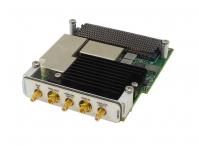
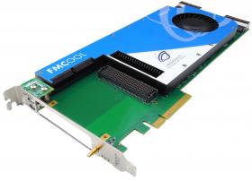
View product FMC263 Data Sheet

FMC268

NEW

FMC ADC 12 bit @ 10.4 GSPS and DAC 16 bit @ 12 GSPS

  • ADC ADC12DJ5200o 8 JESD204C lanes from the ADC is routed to the FMC Connectoro 12-bit @ 10.4 GSPSo Wide full power bandwidth supports IF sampling of signals
  • DAC AD9164/AD9162o 16-bit @ 12 GSPS
  • FPGA Mezzanine Card (FMC) per VITA 57
  • Excellent dynamic performance
  • Front panel interface includes CLK In, Trig In and Trig Out
View product FMC268 Data Sheet

FMC270

NEW

Quad RF 12-GSPS DAC and Quad RF 3-GSPS ADC

  • FPGA Mezzanine Card (FMC) per VITA 57
  • Complete transceiver signal chain solution utilizing Texas Instrument AFE7950
  • Max RF single bandwidth:o 4TX or 2FB: 1200MHz or 2TX:2400MHzo RX: 1200MHz (no FB), 600 MHZ (with FB)
  • RF frequency range:o TX: 600Mhz-12GHzo RX/FB: 600MHz-12GHz
  • Digital step Attenuators
  • Onboard clocking and/or external sampling clock
  • With operation up 12 GHz, the AFE7950 enables direct RF sampling in the L, S, C and X-band frequency ranges without the need for additional frequency conversions stages
  • 29.5Gbs JESD204B/JESD204C digital interface
View product FMC270 Data Sheet

FMC250

FMC Dual ADC 12-bit 2.6 GSPS, Single DAC 16-bit 12 GSPS

  • Dual AD9625 ADC 12-bit at 2.6/2.5/2.0 GSPS
  • 8 JESD204B lanes from each ADC is routed to the FMC+ connector
  • Single DAC AD9164/AD9162 16-bit 12 GSPS
  • FPGA Mezzanine Card (FMC+) per VITA 57.4
  • Excellent dynamic performance
  • Front panel interface includes CLK In, Trig In and Trig Out
View product FMC250 Data Sheet

FMC235

Quad ADC 16-bit @ 250 MSPS, Single DAC 14-bit 500 @ MSPS

  • Dual ADS42JB69 (Quad ADC in total), 16-bit @ 250MSPS
  • JESD204B lanes from each ADC
  • Single DAC3171 (LVDS Based), 14-bit @ 500MSPS
  • Front end RF is DC coupled for the ADC and the DAC
  • Excellent dynamic performance
  • Front panel interface includes CLK In, Trig In and Trig Out
View product FMC235 Data Sheet

FMC255

High-Speed High-Density Single DAC with 8 ADC, FMC

  • Dual LTC2107 ADC 16-bit at 210 MSPS
  • Single LTC2000-16 DAC 16-bit at 1.25 GSPS
  • Dual AD9653 ADC 16-bit at 125 MSPS (total of six channel routed to the front)
  • Front-panel clock and trigger inputs
  • I/O via Ganged Micro RF connector
View product FMC255 Data Sheet

FMC220

Dual 12-bit 1 GSPS ADC and 16-bit 6 GSPS DAC, FMC

  • Analog Devices AD9234 dual 1 GSPS ADC
  • The Analog inputs for the ADC are DC coupled
  • Analog Devices AD9162/9164 6 GSPS RF DACSupported by DAQ Series™ data acquisition software
    • Update rate up to 12 GSPS in somemodes
    • Up to 7.5 GHz in 2nd and 3rd Nyquist
    • Fast frequency hopping (AD9164)
  • FPGA Mezzanine Card (FMC) per VITA 57
  • Excellent dynamic performance
View product FMC220 Data Sheet

FMC256

QSFP28, Dual ADC, dual DAC plus Digital I/O, FMC

  • Four SERDES to QSFP28 to allow for high-speed multi-protocol communicate via Fiber or Copper
  • On board PLL to lock to input clock for synchronization
  • Two channels SAR ADC based on LTC2378, 20-bit at one MSPS
  • Two channels DAC based on AD5791, 20-bit
  • Four digital Output (could be used for Trig In/Out)
  • Standard VITA 57.1 FMC
View product FMC256 Data Sheet

FMC269

NEW

75 MHz to 6 GHz Quad Versatile Wideband Transceiver (MIMO), FMC

  • FPGA Mezzanine Card (FMC) per VITA 57
  • Complete transceiver signal chain solution using Single Analog Device (ADRV9029)
  • Frequency range 75 MHz to 6 GHz with receiver bandwidth up to 200 MHz and transmitter synthesis bandwidth up to 450 MHz
  • MIMO transceiver is Time Domain Duplex (TDD) for 3G/4G/5G
  • Compatible with Analog Devices design tools for ADRV9029
  • Onboard clocking with multi-card synchronization capability
  • 24.33Gbs JESD204B/JESD204C digital interface
View product FMC269 Data Sheet

FMC267

Single DAC with Quad ADC DC Coupled

  • DAC based on the Texas Instruments DAC3171 device with 14-bit @ 500 MSPS
  • ADC based on the Analog Device AD9268 16-bit @ 125MSPS
  • On board PLL
  • FPGA Mezzanine Card (FMC) per VITA 57
  • Clock input for synchronization via front or rear
View product FMC267 Data Sheet

FMC260

Octal RF Transceiver AD9371

  • FPGA Mezzanine Card (FMC+) per VITA 57.4
  • Octal wideband Transceiver, 300 MHz to 6 GHz, using four AD9371
  • Transmit synthesis bandwidth to 250 MHz
  • Two Observation Receiver, one Sniffer Receiver
  • Clock from onboard Wideband PLL or direct RF clock
    • LMK04821 PLL with 122.88 MHz VCXO
View product FMC260 Data Sheet

FMC227

FMC Dual ADC, 12-bit @ 2.6 GSPS with single DAC 14-bit @ 5.7GSPS

  • Dual AD9625 ADC
    • 4/6 JESD204B lanes from the ADC is routed to the FMC
    • 12-bit @ 2.6 GSPS
    • Wide full power bandwidth supports IF sampling of signals up to 2 GHz
  • Single DAC AD9129 
    • 14-bit @ 5.7 GSPS
  • FPGA Mezzanine Card (FMC) per VITA 57
  • Excellent dynamic performance
  • Front panel interface includes CLK In, Trig In and Trig Out
View product FMC227 Data Sheet

FMC253

FMC 12 GSPS DAC, Dual 2.6 GSPS ADC, 250 MSPS ADC

  • ADC dual channel 14-bit @ 2.6 GSPS (AD9689)
  • DAC 16-bit @ 12 GSPS (AD9164/AD9162)
  • ADC 16-bit @ 250 MSPS (AD9467)
  • FPGA Mezzanine Card (FMC) per VITA 57
  • Front panel interface includes Trig In/Out
  • Clock input for synchronization via front or rear
View product FMC253 Data Sheet

FMC234

FMC ADC 12 bit @ 6.4 GSPS and DAC 16 bit @ 12 GSPS

  • ADC 12-bit @ up to 6.4 GSPS (ADC12DJ3200)
  • The ADC has front end attenuators and amplifiers
  • DAC 16-bit @ up to 12 GSPS (AD9164/AD9162)
  • FPGA Mezzanine Card (FMC) per VITA 57
  • Excellent dynamic performance
  • Front panel interface includes CLK In, Trig In and Trig Out
View product FMC234 Data Sheet

FMC232

70 MHz to 6 GHz Dual Versatile Wideband Transceiver (MIMO), FMC

  • Dual complete transceiver signal chain solution using Analog Devices AD9361 transceiver
  • Frequency range 70 MHz to 6 GHz with instantaneous bandwidth from 200 kHz to 56 MHz
  • MIMO transceiver is Time Domain Duplex (TDD) and Frequency Domain Duplex (FDD) compatible
  • Supported by DAQ Series™ data acquisition software
  • FPGA Mezzanine Card (FMC) per VITA 57
  • Multiplexed 2x RF inputs on each RF channel
  • Onboard clocking or external clock with multi-card synchronization capability
  • Low Pin Count (LPC) 160-pin connector
View product FMC232 Data Sheet

FMC233

FMC Quad ADC 16-bit @ 1 GSPS and Quad DAC 16-bit @ 2.8 GSPS

  • Quad ADC 16-bit @ 1.0 GSPS (ADS54J60) or 16-bit @ 500 MSPS (ADS54J69)
  • Quad DAC 16-bit @ 2.8 GSPS (DAC39J84)
  • FPGA Mezzanine Card (FMC) per VITA 57.1
  • Excellent dynamic performance
  • All I/O (including the RF) are mounted on the back side for expansion to an RF front end module
View product FMC233 Data Sheet

FMC219

FMC High-speed Dual DAC 14-bit at 2.5 GSPS with Wide-band PLL on board

  • FPGA Mezzanine Card (FMC) per VITA 57
  • Dual AD9739 DAC 14-bit at 2.5 GSPS
  • 2 Vpp differential analog output swing
  • Programmable DSP clock
  • Front panel GPIO (5 LVDS, or 10 single ended)
  • Dynamic performance
    • 8 QAM carriers @ 400 MHz IF –71 dBc
    • 16 QAM carriers @ 400 MHz IF –68 dBc
    • 32 QAM carriers @ 400 MHz IF –65 dBc
    • 72 QAM carriers @ 600 MHz IF –61 dBc
  • Single tone NSD @ 2.4 GSPS
    • 166 dBm/Hz @ 100 MHz IF
    • 162 dBm/Hz @ 1 GHz IF
  • Connection via SSMC
    • Analog out
    • Reference clock input
    • TRIG input
View product FMC219 Data Sheet

FMC254

FMC+ Quad ADC 12-bit @ 1.6 GSPS

  • Quad ADC12SJ1600 ADC 12-bit at 1.6GSPS
  • Full-Power input bandwidth: 6GHz
  • 4 JESD204C lanes from each ADC
  • FPGA Mezzanine Card (FMC+) per VITA 57.4
  • Excellent dynamic performance
  • Front panel interface includes CLK In and Trig In
View product FMC254 Data Sheet

FMC214

70 MHz to 6 GHz Dual Versatile Wideband Transceiver (MIMO), FMC

  • Dual complete transceiver signal chain solution using Analog Devices AD9361 transceiver
  • Frequency range 70 MHz to 6 GHz with instantaneous bandwidth from 200 kHz to 56 MHz
  • MIMO transceiver is Time Domain Duplex (TDD) and Frequency Domain Duplex (FDD) compatible
  • Supported by DAQ Series™ data acquisition software
  • FPGA Mezzanine Card (FMC) per VITA 57
  • Multiplexed 2x RF inputs on each RF channel
  • On-board clocking with multi-card synchronization capability
  • Low Pin Count (LPC) 160-pin connector
View product FMC214 Data Sheet

FMC211

FMC High-speed ADC 10-bit at 2.6 GSPS Module

  • FPGA Mezzanine Card (FMC) per VITA-57
  • ADC EV10AS150B  @ 2.6 GSPS
  • 5 GHz Full Power Input Bandwidth (–3dB)
  • True single core architecture (no calibration required)
  • Full scale Analog input Voltage Span 500 mVpp
  • Ultra Low Jitter wideband PLL Synthesizer
  • Option for Direct RF clock sampling or  reference clock input
  • The ADC RF input can be differential or single ended
View product FMC211 Data Sheet

FMC212

Dual ADC 12-bit @ 1.5 GSPS and Dual DAC 16-bit @ 2 8 GSPS, FMC

  • Dual ADC 12-bit @ 1.5 GSPS (EV12AS200AZP)
  • The ADC has Full power input Bandwidth at 1.5 GSPS is 2.3 GHz and very low latency < 5 Clock Cycles
  • Dual DAC 16-bit @ 2.8 GSPS (TI DAC39J82)
  • FPGA Mezzanine Card (FMC) per VITA 57
  • Front panel interface includes RF CLK In, Trig In/Out
View product FMC212 Data Sheet

FMC213

FMC Quad ADC 16-bit @ 250 MSPS, DAC 14-bit @ 5.7 GSPS

  • FPGA Mezzanine Card (FMC) per VITA 57
  • Quad ADC based on ADS42JB69
  • DAC based on AD9129
  • RF front panel reference clock input
  • RoHS compliant
View product FMC213 Data Sheet

FMC215

FMC ADC 12-bit @ 4.0 GSPS and DAC 12-bit @ 4.5 GSPS

  • FPGA Mezzanine Card (FMC) per VITA 57.1
  • TI ADC12J4000 12-bit ADC supports 1-4 GSPS with a full-power input bandwidth of 3.2 GHz
  • E2V EV12DS400 12-bit DAC supports up to 4.5 GSPS with output bandwidth 7 GHz
  • Excellent dynamic performance
  • Front panel interface includes CLK In, Trig In, AnalogIn/Out, and GPIO
  • Ultra-Low Noise Wideband PLL
  • On-chip delay locked loops (DLLs) optimize timing between different clock domains.
View product FMC215 Data Sheet

FMC218

FMC High-speed DAC 14-bit at 2.5 GSPS Module

  • FPGA Mezzanine Card (FMC) per VITA-57
  • Single FMC size
  • Single AD9739 DAC 14-bit at 2.5 GSPS
  • 2 Vpp differential Analog output swing
  • Programmable DSP clock
  • Dynamic performance
    • 8 QAM carriers @ 400 MHz IF –71 dBc
    • 16 QAM carriers @ 400 MHz IF –68 dBc
    • 32 QAM carriers @ 400 MHz IF –65 dBc
    • 72 QAM carriers @ 600 MHz IF –61 dBc
  • Single tone NSD @ 2.4 GSP
    • 166 dBm/Hz @ 100 MHz IF
    • 162 dBm/Hz @ 1 GHz IF
  • Connection via MMCX
    • Analog out
    • Reference clock input
    • TRIG input
    • TRIG output
    • GPIO
View product FMC218 Data Sheet

FMC221

FMC DAC 14-bit @ 2.5 GSPS Module

  • FPGA Mezzanine Card (FMC) Per VITA-57
  • AD9739 DAC 14-bit 2.5GSPS
  • Dynamic performanceo
    • 8 QAM carriers @ 400 MHz IF –71 dBco
    • 16 QAM carriers @ 400 MHz IF –68 dBco
    • 32 QAM carriers @ 400 MHz IF –65 dBco
    • 72 QAM carriers @ 600 MHz IF –61 dBc
  • Single tone NSD @ 2.4 GSPSo 166 dBm / Hz @ 100 MHz IFo 162 dBm / Hz @ 1 GHz IF
  • Excellent dynamic performance
  • Front panel interface includes CLK In, Trig In and Trig Out
View product FMC221 Data Sheet

FMC222

Dual DAC 14-bit @ 2.5 GSPS, FMC

  • FPGA Mezzanine Card (FMC) per VITA 57
  • Dual DAC 14-bit @ 2.5 GSPS (AD9739)
  • 2Vpp Differential Analog Output Swing
  • Programmable DSP Clock
  • Dynamic performance:
    • 8 QAM carriers @ 400MHz IF: -71dBc
    • 16QAM carriers @ 400MHz IF: -68dBc
    • 32QAM carriers @ 400MHz IF: -65dBc
    • 72QAM carriers @ 600MHz IF: -61DbC
  • Single Tone NSD @ 2.4GSPS:
    • 166 dBm/Hz @ 100MHz IF
    • 162 dBm/Hz @ 1 GHz IF
  • Trig In/Out
View product FMC222 Data Sheet

FMC223

FMC High-speed DAC 14-bit at 2.5 GSPS Module

  • FPGA Mezzanine Card (FMC) per VITA 57
  • Single module  AD9739 DAC 14-bit at 2.5 GSPS
  • 2 Vpp differential Analog output swing
  • Programmable DSP clock
  • Dynamic performance
    • 8 QAM carriers @ 400 MHz IF –71 dBc
    • 16 QAM carriers @ 400 MHz IF –68 dBc
    • 32 QAM carriers @ 400 MHz IF –65 dBc
    • 72 QAM carriers @ 600 MHz IF –61 dBc
  • Single tone NSD @ 2.4 GSPS
    • 166 dBm/Hz @ 100 MHz IF
    • 162 dBm/Hz @ 1 GHz IF
  • Connection via MMCX for Analog Out and Reference Clock Input
  • Connection via LVDS for TRIG In/Out and GPIO
  • RoHS compliant
View product FMC223 Data Sheet

FMC224

Quad DAC 16-bit @ 2.8 GSPS, FMC

  • FPGA Mezzanine Card (FMC) per VITA 57
  • Quad Port DAC 16-bit at 2.8 GSPS (TI DAC39J84)
  • Independent 1x16x Interpolation
  • Independent Complex Mixers with 48-bit NCO/ or +/-xFs/8
  • Sinx/x Correction Filters
  • Digital Summation of Independent Complex Signals
  • Onboard Wideband PLL
  • Trig In/Out
View product FMC224 Data Sheet

FMC225

12-bit 4.0 GSPS ADC and 14-bit 5.7 GSPS DAC, FMC

  • FPGA Mezzanine Card (FMC) per VITA 57
  • TI ADC12J4000 ADC
    • Usable output bandwidth of 800 MHz at 4x decimation and 4000 MSPS
    • Usable output bandwidth of 100 MHz at 32x decimation and 4000 MSPS
    • Bypass Mode for full Nyquist output bandwidth
  • Analog Devices AD9129 DAC
    • DC-to-1.4 GHz in Baseband mode
    • DC-to-1.0 GHz in 2x Interpolation mode
    • 1.4 to 4.2 GHz in Mix-Mode
  • Supported by DAQ Series™ data acquisition software
  • Excellent dynamic performance
  • Front panel interface includes CLK In, Trig In, Analog In/Out, and GPIO
  • Ultra Low-Noise wide-band PLL
  • On-chip delay locked loops (DLLs) optimize timing between different clock domains.
View product FMC225 Data Sheet

FMC226

Dual ADC, 12-bit @ 4.0 GSPS, FMC

  • FPGA Mezzanine Card (FMC) per VITA 57
  • Dual Texas Instruments ADC12J4000 ADC
    • Four JESD204B lanes per ADC are routed to the FMC connector
    • Usable output bandwidth of 800 MHz at 4x decimation and 4000 MSPS
    • Usable output bandwidth of 100 MHz at 32x decimation and 4000 MSPS
  • Supported by DAQ Series™ data acquisition software
  • Excellent dynamic performance
  • Front panel interface includes CLK In, Trig In, Analog In, and GPIO
  • Ultra Low-Noise wide-band PLL
View product FMC226 Data Sheet

FMC228

Quad ADC 12-bit @ 1 GSPS, FMC

  • FPGA Mezzanine Card (FMC) per VITA 57
  • Quad ADC based on AD9234 (1 GSPS or 500 MSPS)
    • Optional decimate-by-2 DDC per channel
    • JESD204B
    • 2 GHz analog input full power bandwidth
  • Option for Direct RF sampling clock via front panel
  • Supported by DAQ Series™ data acquisition software
  • On board wide-band PLL
  • Trig In/Out
  • CLK In
View product FMC228 Data Sheet

FMC210

FMC ADC 10-bit @ 2.6 GSPS Module

  • FPGA Mezzanine Card (FMC) per VITA-57
  • Single ADC EV10AS150B @2.5 GSPS
  • Single module
  • 5 GHz Full Power Input Bandwidth (-3dB)
  • True single core architecture (no calibration required)
  • External Interleaving:Full scale analog input Voltage Span 500mVpp
    • Gain Adjust
    • Offset Adjust
    • Sampling Delay Adjust
  • All front panel input/outputs are via MMCX:
    • Analog Input
    • Reference clock
    • Trig in/out
    • General purpose I/O
  • Super low phase noise RF PLL Synthesizer
View product FMC210 Data Sheet

FMC A/D D/A

( expand all )

FMC252

Dual Channel DC to 9GHz Vector Signal Generator based on AD9166 FMC+

FMC216

ADC 12-bit @ 2.6 GSPS and DAC 14-bit @ 5.6 GSPS, FMC

FMC154

Local Oscillator (LO) with Input Reference, FMC

FMC217

FMC ADC 12-bit @ 6.4 GSPS and DAC 16-bit @ 12 GSPS

FMC231

Quad ADC 16-bit @ 1 GSPS and Quad DAC 16-bit @ 2.8 GSPS, FMC

FMC229

FMC Quad DAC 16-bit @ 2.8 GSPS with Quadrature Modulator

FMC238

75 MHz to 6 GHz Dual Versatile Wideband Transceiver (MIMO), FMC

FMC239

75 MHz to 6 GHz Quad Versatile Wideband Transceiver (MIMO), FMC

FMC251

Dual ADC 2.6 GSPS, ADC 250 MSPS and DAC 12 GSPS, FMC

FMC158

Multi I/O FMC Module, M-LVDS, RS-485/RS-422, GPIO +3.3V/+5V, ADC and DAC

FMC159

Quad channel baseband ADC with Eight RS-485/RS-422

FMC230

MIMO 300 MHz to 6 GHz Octal Versatile Wideband Transceiver FMC

FMC261

Dual ADC 2.6 GSPS, ADC 250 MSPS, DAC 12.6 GSPS, 2x22 Output and 2x1 Input, FMC

FMC262

Quad ADC 14-bit @ 3 GSPS with AD9208 or 2.6 GSPS with AD9689 FMC+

FMC164

Local Oscillator (LO) with Input Reference, FMC

FMC237

75 MHz to 6 GHz Quad Versatile Wideband Transceiver (MIMO), FMC

FMC248

30 MHz to 6 GHz Dual Narrow-Band and Wideband RF Transceiver, FMC

FMC249

30 MHz to 6 GHz Quad Narrow-Band and Wideband RF Transceiver, FMC

FMC263

Mixed Signal Front End with Quad RF DAC and Quad RF ADC

FMC268

FMC ADC 12 bit @ 10.4 GSPS and DAC 16 bit @ 12 GSPS

FMC270

Quad RF 12-GSPS DAC and Quad RF 3-GSPS ADC

FMC250

FMC Dual ADC 12-bit 2.6 GSPS, Single DAC 16-bit 12 GSPS

FMC235

Quad ADC 16-bit @ 250 MSPS, Single DAC 14-bit 500 @ MSPS

FMC255

High-Speed High-Density Single DAC with 8 ADC, FMC

FMC220

Dual 12-bit 1 GSPS ADC and 16-bit 6 GSPS DAC, FMC

FMC256

QSFP28, Dual ADC, dual DAC plus Digital I/O, FMC

FMC269

75 MHz to 6 GHz Quad Versatile Wideband Transceiver (MIMO), FMC

FMC267

Single DAC with Quad ADC DC Coupled

FMC260

Octal RF Transceiver AD9371

FMC227

FMC Dual ADC, 12-bit @ 2.6 GSPS with single DAC 14-bit @ 5.7GSPS

FMC253

FMC 12 GSPS DAC, Dual 2.6 GSPS ADC, 250 MSPS ADC

FMC234

FMC ADC 12 bit @ 6.4 GSPS and DAC 16 bit @ 12 GSPS

FMC232

70 MHz to 6 GHz Dual Versatile Wideband Transceiver (MIMO), FMC

FMC233

FMC Quad ADC 16-bit @ 1 GSPS and Quad DAC 16-bit @ 2.8 GSPS

FMC219

FMC High-speed Dual DAC 14-bit at 2.5 GSPS with Wide-band PLL on board

FMC254

FMC+ Quad ADC 12-bit @ 1.6 GSPS

FMC214

70 MHz to 6 GHz Dual Versatile Wideband Transceiver (MIMO), FMC

FMC211

FMC High-speed ADC 10-bit at 2.6 GSPS Module

FMC212

Dual ADC 12-bit @ 1.5 GSPS and Dual DAC 16-bit @ 2 8 GSPS, FMC

FMC213

FMC Quad ADC 16-bit @ 250 MSPS, DAC 14-bit @ 5.7 GSPS

FMC215

FMC ADC 12-bit @ 4.0 GSPS and DAC 12-bit @ 4.5 GSPS

FMC218

FMC High-speed DAC 14-bit at 2.5 GSPS Module

FMC221

FMC DAC 14-bit @ 2.5 GSPS Module

FMC222

Dual DAC 14-bit @ 2.5 GSPS, FMC

FMC223

FMC High-speed DAC 14-bit at 2.5 GSPS Module

FMC224

Quad DAC 16-bit @ 2.8 GSPS, FMC

FMC225

12-bit 4.0 GSPS ADC and 14-bit 5.7 GSPS DAC, FMC

FMC226

Dual ADC, 12-bit @ 4.0 GSPS, FMC

FMC228

Quad ADC 12-bit @ 1 GSPS, FMC

FMC210

FMC ADC 10-bit @ 2.6 GSPS Module

MicroTCA.4 AD/DA

( close )

MRT523

MTCA.4 RTM for AMC523, 12 Ch ADC 16-bit @ 125 MSPS

  • MicroTCA.4 RTM for the AMC523
  • Twelve channel ADC 16-bit @ 125 MSPS utilizing AD9653 device routed to AMC523
  • Two analog outputs from AMC523’s DACs Mezzanine
  • ADC and DAC signal routed through amezzanine
  • Three pairs of user defined digital I/O
  • Double module, mid-size (full-size optional)
View product MRT523 Data Sheet

AMC523

Dual DAC 16-bit @ 250 MSPS, Kintex-7, MTCA.4

  • Dual DAC 16-bit @ 250 MSPS utilizing MAX5878 device (user programmable for lower sampling rate)
  • Xilinx Kintex-7 FPGA XC7K410T in FFG900 package
  • Supported by DAQ Series™ data acquisition software
  • 2 GB of DDR3 memory
  • Internal clock or precision external clock from RTM/backplane/front panel clocks
  • Trig in/out configurable by software (external trigger via front or port 17)
  • x8 PCIe (or dual x4)
  • AMC FCLKA, TCLKA, TCLKB, TCLKC and TCLKD are routed
  • Quad SFP+ (up to 6.6 Gbps)
  • JTAG selectable front and backplane
View product AMC523 Data Sheet

MRT575A

MTCA.4 RTM for AMC575, Passive

  • MicroTCA.4 RTM for the AMC575
  • 8 ADC and 16 DAC signals routed to rear panel
  • Clock/trigger routed to rear panel
View product MRT575A Data Sheet

MRT566A

MTCA.4 RTM for AMC566

  • MicroTCA.4 RTM for the AMC566
  • DESY D1.4 Specification
  • 4x TI ADS42JB69
  • Total of 8 ADC 16-bit @ 250MSPS
  • Clock input for synchronization
View product MRT566A Data Sheet

MRT577A

MTCA.4 RTM for AMC577

  • MicroTCA.4 RTM for the AMC577
  • 16 ADC and input via Balun
  • 16 DAC as output via Balun
View product MRT577A Data Sheet

AMC522

MTCA.4 AMC Dual DAC, 16-bit @ 250 MSPS

  • Dual channel DAC 16-bit @ 250 MSPS (MAX5878)
  • Compliant to MTCA.4, double module, mid-size (full-size optional) with rear I/O
  • Xilinx Kintex-7 FPGA
  • Dual PCIe x4 or PCIe x8
  • JTAG interface port
  • AMC.1, AMC.2, AMC.4 compliant (FPGA programmable)
  • IPMI v2.0 compliant
View product AMC522 Data Sheet

MRT522

MTCA.4 RTM for AMC522

  • Double module, mid-size (full-size optional)
  • Two analog outputs from AMC522’s DACs via SSMC connectors
  • Eight analog inputs (AC or DC coupled) via SSMC connectors feeding on-board ADCs via programmable gain amplifiers JTAG interface port
  • Clocks and Trigger In/Out accessible via  Mini-display Port connectors
  • IPMI v2.0 compliant
View product MRT522 Data Sheet

MRT520

MicroTCA.4 RTM for AMC520

  • MicroTCA.4 RTM for the AMC520
  • Two analog outputs from AMC520’s DACs via SSMC connectors
  • Ten analog inputs (AC or DC coupled) interfacing directly with AMC520’s ADC ICs via SSMC connectors
  • Twelve LVDS signals and three differential reference clock routing to AMC520’s FPGA
  • LVDS and reference clocks accessible via dual high density DensiShield connectors
  • Double module, mid-size (full-size optional)
  • RoHS compliant
View product MRT520 Data Sheet

AMC521

24 Channels ADC, Mixed Sampling Rate

  • Sixteen channel of TI ADS42JB69 ADC 16-bit @ 250 MSPS
  • Eight channel SAR TI ADS8568 ADC 16-bit @ 650 KSPS simultaneous
  • Interface to the FPGA via JESD204B
  • 24 LVDS for Clock/Trig and/or GPIO
  • Virtex-7 FPGA 415T or 690T in FFG1158
  • Internal/External clock
  • Clock Jitter Cleaner with Dual Loop PLLs
  • Trig In/Out
  • A/D input via SSMC connectors
View product AMC521 Data Sheet

AMC520

AMC 10-channel ADC, MicroTCA.4

  • Double module AMC, compliant to μTCA.4
  • Ten channel of ADC with 125MSPS @ 16-bit resolution utilizing AD9268 device
  • Dual DAC with 250 MSPS @ 16-bit resolution utilizing MAX5878 device (this is user programmable for lower sampling rate)
  • Internal clock or precision external clock from RTM/backplane/front panel clocks
  • Trig in/out configurable by software (external trigger via front or port 17)
  • Backplane PCIe Dual x4 or x8/Dual GbE
  • Xilinx Virtex-6 FPGA in FF1759 package
  • Option for QDR-II+
  • AMC FCLKA, TCLKA, TCLKB, TCLKC and TCLKD are routed
  • Dual SFP+ (up to 6.6Gbps)
  • JTAG selectable front and backplane
  • AMC.1 and AMC.2 (FPGA programmable)
View product AMC520 Data Sheet

MicroTCA.4 AD/DA

( expand all )

MRT523

MTCA.4 RTM for AMC523, 12 Ch ADC 16-bit @ 125 MSPS

AMC523

Dual DAC 16-bit @ 250 MSPS, Kintex-7, MTCA.4

MRT575A

MTCA.4 RTM for AMC575, Passive

MRT566A

MTCA.4 RTM for AMC566

MRT577A

MTCA.4 RTM for AMC577

AMC522

MTCA.4 AMC Dual DAC, 16-bit @ 250 MSPS

MRT522

MTCA.4 RTM for AMC522

MRT520

MicroTCA.4 RTM for AMC520

AMC521

24 Channels ADC, Mixed Sampling Rate

AMC520

AMC 10-channel ADC, MicroTCA.4

Platform A/D D/A

( close )

VT988

High speed 16 ADC @ 3 GSPS with Synchronous Capture

  • 16 ADC for synchronous capture
  • Xilinx Virtex-7 XC7VX485T FPGA
  • NVidia Jetson TX2 System on Module
  • 8-bit @ 3 GSPS (TI ADC08B3000)
  • Managed Layer 2 GbE Switch
View product VT988 Data Sheet

VT981

3rd Generation RFSoC w/ XCVU13P FPGA and RF/IF carrier

  • 8 ADC / 8 DAC simultaneous processing
  • 3rd Generation Xilinx RFSoC XCZU47DR
    • 16GB of DDR4
  • Suitable for 5G, 4G, LET and SDR deployment
  • FPGA data processing w/ Xilinx Virtex UltraScale+ XCVU13P
    • 16GB of DDR4
  • FMC+ socket for addition RF and I/O
    • The FMC+ could extend beyond the FMC+ in length for added real estate (up to XMC size is supported) 
  • Accommodate 3rd party RF/IF daughter card
    • Accomplished thru an FMC connector to the RF Module
  • Clock and Timing Synchronization to the RF/IF
View product VT981 Data Sheet

VT983

Quad ADC @ 250 MSPS and Single DAC @ 250 MSPS

  • Quad ADC 16-bit @ 250 MSPS for synchronous capture (TI ADS42LB69)
  • Single DAC 16-bit @ 250 MSPS (Maxim MAX5878)
  • Xilinx Virtex-7 690T FPGA
  • NVidia Jetson TX2 System on Module
  • Managed Layer two GbE Switch
View product VT983 Data Sheet

Platform A/D D/A

( expand all )

VT988

High speed 16 ADC @ 3 GSPS with Synchronous Capture

VT981

3rd Generation RFSoC w/ XCVU13P FPGA and RF/IF carrier

VT983

Quad ADC @ 250 MSPS and Single DAC @ 250 MSPS

VPX FPGA A/D D/A

( close )

VPX597

300 MHz to 6 GHz Octal Versatile Wideband Transceiver (MIMO), Kintex UltraScale™, 3U VPX

  • Xilinx Kintex UltraScale™ XCKU115 FPGA
  • Four AD9371s or AD9375s on one module
  • Octo complete transceiver signal chain solution
  • Tx synthesis bandwidth to 250 MHz
  • Rx bandwidth: 8 MHz to 100 MHz
  • Health Management through dedicated Processor
View product VPX597 Data Sheet

VPX588

Quad ADC @ 3 GSPS with Quad DAC @ 12 GSPS, Virtex UltraScale+™, 3U VPX

  • Xilinx UltraScale+™ XCVU13P FPGA
  • Quad ADC 14-bit @ 3 GSPS (AD9208)
  • Quad DAC 16-bit @ 12 GSPS (AD9162 or AD9164)
  • Single bank of DDR4 64-bit wide 8 GB Total
  • 16 SERDES as PCIe/SRIO/10GbE/40GbE/Aurora to P1
  • 8 SERDES as PCIe/SRIO/10GbE/40GbE/Aurora to P2
  • Clock Jitter cleaner
  • Option for Direct RF Clock sampling for the ADC/DAC
  • Health Management through dedicated Processor
View product VPX588 Data Sheet

VPX589

Dual ADC @ 6.4 GSPS and Dual DAC @ 12 GSPS, Virtex UltraScale+™, 3U VPX

  • Xilinx Virtex UltraScale+™ XCVU13P FPGA
  • Dual ADC 12-bit @ 10.4/6.4 GSPS or quad ADC @ 5.2/3.2 GSPS with TI ADC12DJ5200 or ADC12DJ3200
  • Option for ADC12DJ5200, ADC12DJ3200 or ADC12DJ2700
  • Dual DAC 16-bit @ 12 GSPS (AD9162 or AD9164)
  • 16 SERDES as PCIe/SRIO/10GbE/40GbE/Aurora to P1
  • 8 SERDES as PCIe/SRIO/10GbE/40GbE/Aurora to P2
  • Clock Jitter cleaner
  • Option for Direct RF Clock sampling for the ADC/DAC
  • Single bank of DDR4 64-bit wide 8 GB Total
  • Health Management through dedicated Processor
View product VPX589 Data Sheet

VPX587

300 MHz to 6 GHz Octal Versatile Wideband Transceiver (MIMO), Virtex UltraScale+™, 3U VPX

  • Xilinx Virtex UltraScale+™ XCVU13P FPGA
  • Four AD9371s or AD9375s on one module
  • Octo complete transceiver signal chain solution
  • Tx synthesis bandwidth to 250 MHz
  • Rx bandwidth: 8 MHz to 100 MHz
  • Health Management through dedicated Processor
View product VPX587 Data Sheet

VPX572

Dual ADC 12-bit @ 6.4 GSPS or Quad ADC @ 3.2 GSPS Virtex UltraScale+, 3U VPX

  • Dual ADC 12-bit @ 6.4 GSPS (ADC12DJ3200) or Quad ADC @ 3.2 GSPS
  • Health Management through dedicated Processor
View product VPX572 Data Sheet

VPX582

NEW

Integrated Octal RF Transceiver in 3U VPX

  • Octal RF transceiver utilizing AD9371 and/or AD9375
  • Xilinx UltraScale+ XCZU15EG FPGA
  • 8 GB of 64-bit wide DDR-4 Memory with ECC to ARM
  • 8 GB of 64-bit wide DDR-4 Memory to FPGA
  • MPSoC with block RAM and UltraRAM
  • Health Management through dedicated Processor
View product VPX582 Data Sheet

VPX599

Dual ADC @ 6.4 GSPS and Dual DAC @ 12 GSPS, UltraScale™, 3U VPX

  • 3U FPGA Dual ADC and Dual DAC per VITA 46
  • Xilinx Kintex UltraScale™ XCKU115 FPGA
  • Dual ADC 12-bit @ 6.4 GSPS or quad ADC at 3.2 GSPS with TI ADC12DJ3200
  • Option for ADC12DJ3200 or ADC12DJ2700
  • Dual DAC 16-bit @ 12 GSPS (AD9162 or AD9164) or TI DAC38RF82 14-bit @ 9GSPS
  • High-performance clock jitter cleaner
  • VHDL reference design with source code
  • Protocols such as PCIe, SRIO, 10GbE/40GbE, etc. are FPGA programmable
  • 16 GB of DDR4 Memory (64-bit wide)
  • Health Management through dedicated Processor
View product VPX599 Data Sheet

VPX598

Quad DAC @ 12 GSPS with Quad ADC @ 3 GSPS, Kintex UltraScale™, 3U VPX

  • 3U FPGA Quad DAC and Quad ADC per VITA 46
  • Xilinx Kintex UltraScale™ XCKU115 FPGA
  • Quad ADC channels (AD9208) 14-bits @ 3 GSPS
  • Quad DAC channels (AD9162 or AD9164) 16-bits @ 12 GSPS
  • Two banks of 64-bit wide DDR4 for a total of 16 GB
  • Health Management through dedicated Processor
View product VPX598 Data Sheet

VPX570

ADC 12-bit @ 5.4 GSPS and DAC 12-bit @ 6 GSPS, Virtex UltraScale+, 3U VPX

  • ADC 12-bit @ 5.4 GSPS (EV12AS350A)
  • DAC 12-bit @ 6 GSPS (EV12DS460A)
  • RF switch to loop the DAC to ADC
  • Xilinx UltraScale+ XCVU13P FPGA with 8 GB DDR4
  • Supported by development accelerator software package for Multi-Path Modulation
  • Health Management through dedicated Processor
View product VPX570 Data Sheet

VPX571

Dual RF Agile Transceiver with VITA 67.2 RF Connector, 3U VPX

  • Dual RF transceiver (AD9364)
  • Xilinx UltraScale+ XCZU15EG FPGA
  • 8 GB of 64-bit wide DDR4 Memory (single bank) with ECC
  • MPSoC with block RAM and UltraRAM
  • RF routed as option to VITA 67.2
  • Health Management through dedicated Processor
View product VPX571 Data Sheet

MPM_VPX570

Development Accelerator “Multi-Path Modulation” Software Package

  • Loopback pipeline ADC-DAC
  • Quadrature Generator
  • Multi-Path with N independent branches
  • N independent variable delays and gain
  • N independent Phase and Amplitude modulators
  • Combiner for N branches
  • MATLAB® model included
View product MPM_VPX570 Data Sheet

VPX574

Dual RF Agile Transceiver with Front I/O, 3U VPX

  • Dual RF transceiver (AD9364)
  • Xilinx UltraScale+ XCZU15EG FPGA
  • 8 GB of 64-bit wide DDR4 Memory (single bank) with ECC
  • MPSoC with block RAM and UltraRAM
  • Health Management through dedicated Processor
View product VPX574 Data Sheet

VPX576

Virtex UltraScale+ FPGA with Octal ADC/DAC in 6U VPX

  • Xilinx XCVU13P UltraScale+
  • Two banks of DDR4 Memory 16GB totalo
    • Single Bank of 64-bit wide 8G
    • Bo Single Bank of 32-bit wide 4GB
  • Four QSFP28 (4x 100GbE)
  • Dual Analog Device AD9081o 8 ADC/DAC fully synchronizedo Direct RF CLK
  • Xilinx Zynq UltraScale+ XCZU04CG
  • 8GB of DDR4 with ECC
  • 64GB of SSD
  • Health Management through dedicated Processor
View product VPX576 Data Sheet

VPX578

3rd Generation Zynq RFSoC UltraScale+, 6U VPX

  • 3rd Generation Xilinx RFSoC XCZU47DR
  • 8 ADC and 8 DAC simultaneous processing
  • Suitable for 5G/4G/LTE and SDR deployment
  • 8GBytes of DDR-4 with ECC to PS
  • 8GBytes of DDR-4 to PL
  • MPSoC with block RAM and UltraRAM
  • 64G SATA NANDrive
  • 32 GPIO, 20 LVDS and 4x RS-485
  • Health Management through dedicated Processor
View product VPX578 Data Sheet

VPX579

3rd Generation Zynq RFSoC UltraScale+, 6U VPX

  • 3rd Generation Xilinx RFSoC XCZU49DR
  • 16 ADC and 16 DAC simultaneous processing
  • Suitable for 5G/4G/LTE and SDR deployment
  • 8GBytes of DDR-4 with ECC to PS
  • 8GBytes of DDR-4 to PL
  • MPSoC with block RAM and UltraRAM• 64G SATA NANDrive
  • 32 GPIO, 20 LVDS and 4x RS-485
  • Health Management through dedicated Processor
View product VPX579 Data Sheet

VPX584

Four ADC 12-bit @ 10.25 GSPS with UltraScale+, 3U VPX

  • Four ADC 12-bit @ 10.25 GSPS
  • Utilizing Analog Device AD9213
  • Xilinx UltraScale+ XCVU13P FPGA
  • High speed SERDES to the P1/P2
  • Dual 64-bit wide bank of DDR4 with a total of 16GB
  • Supported by development accelerator software
  • Health Management through dedicated Processor
View product VPX584 Data Sheet

VPX FPGA A/D D/A

( expand all )

VPX597

300 MHz to 6 GHz Octal Versatile Wideband Transceiver (MIMO), Kintex UltraScale™, 3U VPX

VPX588

Quad ADC @ 3 GSPS with Quad DAC @ 12 GSPS, Virtex UltraScale+™, 3U VPX

VPX589

Dual ADC @ 6.4 GSPS and Dual DAC @ 12 GSPS, Virtex UltraScale+™, 3U VPX

VPX587

300 MHz to 6 GHz Octal Versatile Wideband Transceiver (MIMO), Virtex UltraScale+™, 3U VPX

VPX572

Dual ADC 12-bit @ 6.4 GSPS or Quad ADC @ 3.2 GSPS Virtex UltraScale+, 3U VPX

VPX582

Integrated Octal RF Transceiver in 3U VPX

VPX599

Dual ADC @ 6.4 GSPS and Dual DAC @ 12 GSPS, UltraScale™, 3U VPX

VPX598

Quad DAC @ 12 GSPS with Quad ADC @ 3 GSPS, Kintex UltraScale™, 3U VPX

VPX570

ADC 12-bit @ 5.4 GSPS and DAC 12-bit @ 6 GSPS, Virtex UltraScale+, 3U VPX

VPX571

Dual RF Agile Transceiver with VITA 67.2 RF Connector, 3U VPX

MPM_VPX570

Development Accelerator “Multi-Path Modulation” Software Package

VPX574

Dual RF Agile Transceiver with Front I/O, 3U VPX

VPX576

Virtex UltraScale+ FPGA with Octal ADC/DAC in 6U VPX

VPX578

3rd Generation Zynq RFSoC UltraScale+, 6U VPX

VPX579

3rd Generation Zynq RFSoC UltraScale+, 6U VPX

VPX584

Four ADC 12-bit @ 10.25 GSPS with UltraScale+, 3U VPX

ATCA RF Systems

ATC500

Base Board for Wideband Massive MIMO Software Defined Radio

  • Dual Virtex UltraScale+ VU13P provides massive DSP power using over 24,000 FPGA DSP slices to deliver up to 12TMACs per second/per board
  • Backplane connections support full mesh fabric at 100G
  • Network synchronization distributes reference and radio frame clocks across multiple ATC500 boards
  • Built-in TX and RX reference for antenna port phase alignment and calibration to support massive MIMO
  • Highly integrated patent-pending radio modules built using four ADRV9009 enhanced by RF DSPs advanced algorithms
  • Each board supports dual high-performance radio modules and scalable to 12 boards with super low jitter among all RF ports
View product ATC500 Data Sheet

ATCA RF Systems

( expand all )

ATC500

Base Board for Wideband Massive MIMO Software Defined Radio

SOFI A/D D/A

( close )

SOF202

Dual ADC @ 6.4 GSPS, Direct RF Clocking, SOFI Module

  • Dual ADC 12-bit @ 6.4 GSPS (dual ADC12DJ3200), supports four channels @ 3.2 GSPS
  • Dual DAC 16-bit @ 12 GSPS (dual AD9162 or AD9164), supports 6 GHz direct RF synthesis
  • Direct front-panel clocking of ADCs/DACs
View product SOF202 Data Sheet

SOF203

Quad ADC and quad DAC, SOFI Module

  • Quad ADC 14-bit @ 3 GSPS (dual AD9208), with option to support up to eight channels*
  • Quad DAC 16-bit @ 12 GSPS (quad AD9162 or AD9164), with option to support up to eight channels*
  • Separate direct front-panel clocking for ADC and DAC
  • Onboard clock buffers with ultralow phase noise

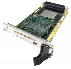
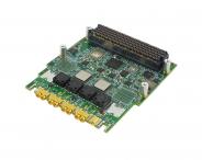
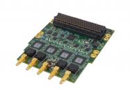
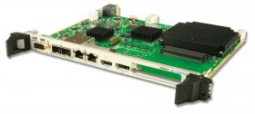
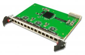
(*See applicable AMC/VPX product datasheet for details)

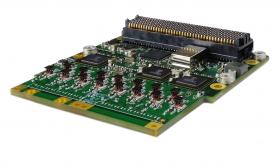
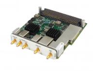
View product SOF203 Data Sheet

SOF205

Quad ADC and quad DAC, SOFI Module

  • Quad ADC 14-bit @ 3 GSPS (dual AD9208)
  • Quad DAC 16-bit @ 12 GSPS (quad AD9162 or AD9164)
  • Onboard Wideband PLL structure
  • LMK04821/8 PLL (with 100 MHz VCXO) for JESD lane clocking and sysref
View product SOF205 Data Sheet

SOF209

Quad ADC 14-bit @ 3 GSPS, SOFI Module

  • Quad ADC 14-bit @ 3 GSPS (dual AD9208)
  • Optional additional quad ADC using a further two AD9208
  • Onboard Wideband PLL structure
  • LMK04821 PLL (with 100 MHz VCXO) for JESD lane clocking and sysref
View product SOF209 Data Sheet

SOF217

Dual ADC @ 6.4 GSPS, SOFI Module

  • Dual ADC 12-bit @ 6.4 GSPS (dual ADC12DJ3200), supports four channels @ 3.2 GSPS
  • Dual DAC 16-bit @ 12 GSPS (dual AD9162 or AD9164), supports 6 GHz direct RF synthesis
  • Sampling clock from host module
  • Onboard Wideband PLL structure
  • LMK04828 PLL (with 100 MHz VCXO) for JESD lane clocking and sysref
View product SOF217 Data Sheet

SOF218

Quad ADC 14-bit @ 3 GSPS, Programmable Attenuator, SOFI Module

  • Quad ADC 14-bit @ 3 GSPS (dual AD9208)
  • Programmable attenuation on RF inputs
  • Optional additional quad ADC using a further two AD9208
  • Onboard Wideband PLL structure
  • LMK04821 PLL (with 100 MHz VCXO) for JESD lane clocking and sysref
View product SOF218 Data Sheet

SOF219

Quad DAC, SOFI Module

  • Quad DAC (AD9162) with programmable output Attenuation
  • LMK04832 PLL
  • LXM2592 PLL
View product SOF219 Data Sheet

SOF206

NEW

Dual ADC @ 6.4 GSPS with Dual DAC at 9 GSPS with Direct RF Clock Input, SOFI Module

  • Dual ADC 12-bit @ 6.4 GSPS (dual ADC12DJ3200), supports four channels @ 3.2 GSPS
  • Dual DAC 9-bit @ 9 GSPS TI DAC38RF82
  • Direct RF Clock input
View product SOF206 Data Sheet

SOF220

Quad ADC 12-bit @ 1.6 GSPS, SOFI Module

  • Quad ADC12SJ1600 ADC 12-bit at 1.6GSPS
  • Full-Power input bandwidth: 6 GHz
  • 4 JESD204C lanes from each ADC
  • Onboard Wideband PLL
  • LMK04832 PLL (with 100 MHz VCXO)
View product SOF220 Data Sheet

SOF200

Dual ADC @ 6.4 GSPS, SOFI Module

  • Dual ADC 12-bit @ 6.4 GSPS (dual ADC12DJ3200), supports four channels @ 3.2 GSPS
  • Dual DAC 16-bit @ 12 GSPS (dual AD9162 or AD9164), supports 6 GHz direct RF synthesis
  • Sampling clock from host module
  • Onboard Wideband PLL structure
  • LMK04821 PLL (with 100 MHz VCXO)
View product SOF200 Data Sheet

SOF201

Octal RF Transceiver, SOFI Module

  • Octal wideband Transceiver, 300 MHz to 6 GHz, using four AD9371
  • Transmit synthesis bandwidth to 250 MHz
  • Two Observation Receiver, one Sniffer Receiver
  • Clock from onboard Wideband PLL or direct RF clock
  • LMK04821 PLL with 122.88 MHz VCXO
View product SOF201 Data Sheet

SOF207

Quad ADC @ 3GSPS, Direct RF Clocking, SOFI Module

  • Quad ADC 14-bit @ 3 GSPS (dual AD9208)
  • Optional additional quad ADC using a further two AD9208
  • Direct front-panel clocking of ADCs
View product SOF207 Data Sheet

SOF208

Dual ADC @ 6.4 GSPS and Dual DAC 16-bit @ 12 GSPS

  • Dual ADC 12-bit @ 6.4 GSPS (dual ADC12DJ3200), supports four channels @ 3.2 GSPS
  • Dual DAC 9-bit @ 9 GSPS TI DAC38RF82
  • Sampling clock from host module
  • Onboard Wideband PLL structure
  • LMK04821 PLL (with 100 MHz VCXO)
View product SOF208 Data Sheet

SOF221

Dual ADC @ 10.4 GSPS SOFI Module

  • Dual ADC 12-bit @ 10.4 GSPS (dual ADC12DJ5200), supports four channels @ 5.2 GSPS
  • Dual DAC 16-bit @ 12 GSPS (dual AD9162 or AD9164), supports 6 GHz direct RF synthesis
  • Sampling clock from host module
  • Onboard Wideband PLL structure
  • LMK04828 PLL (with 100 MHz VCXO) for JESD lane clocking and sysref
View product SOF221 Data Sheet

SOFI A/D D/A

( expand all )

SOF202

Dual ADC @ 6.4 GSPS, Direct RF Clocking, SOFI Module

SOF203

Quad ADC and quad DAC, SOFI Module

SOF205

Quad ADC and quad DAC, SOFI Module

SOF209

Quad ADC 14-bit @ 3 GSPS, SOFI Module

SOF217

Dual ADC @ 6.4 GSPS, SOFI Module

SOF218

Quad ADC 14-bit @ 3 GSPS, Programmable Attenuator, SOFI Module

SOF219

Quad DAC, SOFI Module

SOF206

Dual ADC @ 6.4 GSPS with Dual DAC at 9 GSPS with Direct RF Clock Input, SOFI Module

SOF220

Quad ADC 12-bit @ 1.6 GSPS, SOFI Module

SOF200

Dual ADC @ 6.4 GSPS, SOFI Module

SOF201

Octal RF Transceiver, SOFI Module

SOF207

Quad ADC @ 3GSPS, Direct RF Clocking, SOFI Module

SOF208

Dual ADC @ 6.4 GSPS and Dual DAC 16-bit @ 12 GSPS

SOF221

Dual ADC @ 10.4 GSPS SOFI Module

VME A/D D/A

VME599

Quad ADC @ 3.2 GSPS or Dual ADC @ 6.4 GSPS, FPGA Kintex UltraScale

  • VME open standard form factor
  • FPGA Xilinx UltraScale™ XCKU115
  • ADC based on TI ADC12DJ3200
    • Quad 3.2 GSPS or Dual 6.4 GSPS
  • Dual 10GbE to FPGA
  • Dual bank of x64 DDR-4 and Single bank of x32 DDR-4 to FPGA
  • GbE to FPGA
  • Quad Core ARM CortexA53 at 1.6GHz per core
  • GbE to ARM
  • 4GB x32 DDR4 to ARM
  • LVDS to backplane to P0
View product VME599 Data Sheet

VME A/D D/A

( expand all )

VME599

Quad ADC @ 3.2 GSPS or Dual ADC @ 6.4 GSPS, FPGA Kintex UltraScale